Commercial use of this content is strictly prohibited. For more details on licensing policy, please visit the About page.
1. Fundamental Concepts
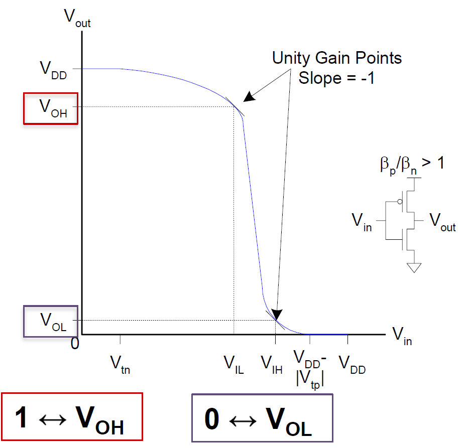
1.1 Voltage Transfer Characteristic (VTC)
Relationship between input voltage and output voltage .
Example:
VTC of a CMOS Inverter
There’re some symbols need to be explained:
= minimum HIGH input voltage
=maximum LOW input voltage
=minimum HIGH output voltage
=maximum LOW output voltage
is a function of .
If we connect the output end and the input end, we get a
The is called switching threshold voltage.
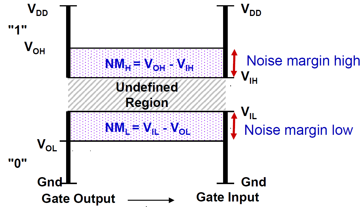
1.2 Noise Margin
Difference between the minimum HIGH output voltage of driving gate and the minimum HIGH input voltage recognized by receiving gate.
For low flatten, the same.
Noise Margin of a Inverter
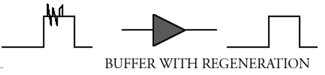
1.3 Regenerative Property
The ability of a CMOS inverter to recover the input unideal digital signal to an approximate ideal signal.
What is Regenerative Property
This characteristic derives from two main reasons:
VTC: curve is very stiff in undefined region. Small disturbance will cause the signal to leave the undefined region.
Push-Pull Output: CMOS inverter has high input resistance (MOS Gates are insulated) and low output resistance (MOS Source-Drain resistance in saturation area is small). The output end is connected with VDD or GND through a very small resistance.
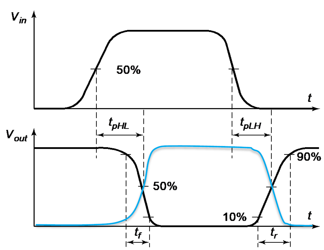
1.4 Delay Definitions
: response time of the gate for a low to high (or positive) output transition.
: response time of the gate for a high to low (or negative) output transition.
Note that the LH or HL is determined by the output direction.
i.e.,
If the output falls from high to low,
the delay time is ,
and vice versa.
and
Propagation delay time:
Contamination delay time:
Fall time: 90% - 10% voltage point
Rise time: 10% - 90% voltage point
Fall Time and Rise Time
2. Diodes
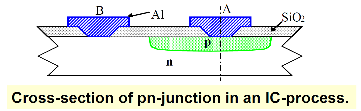
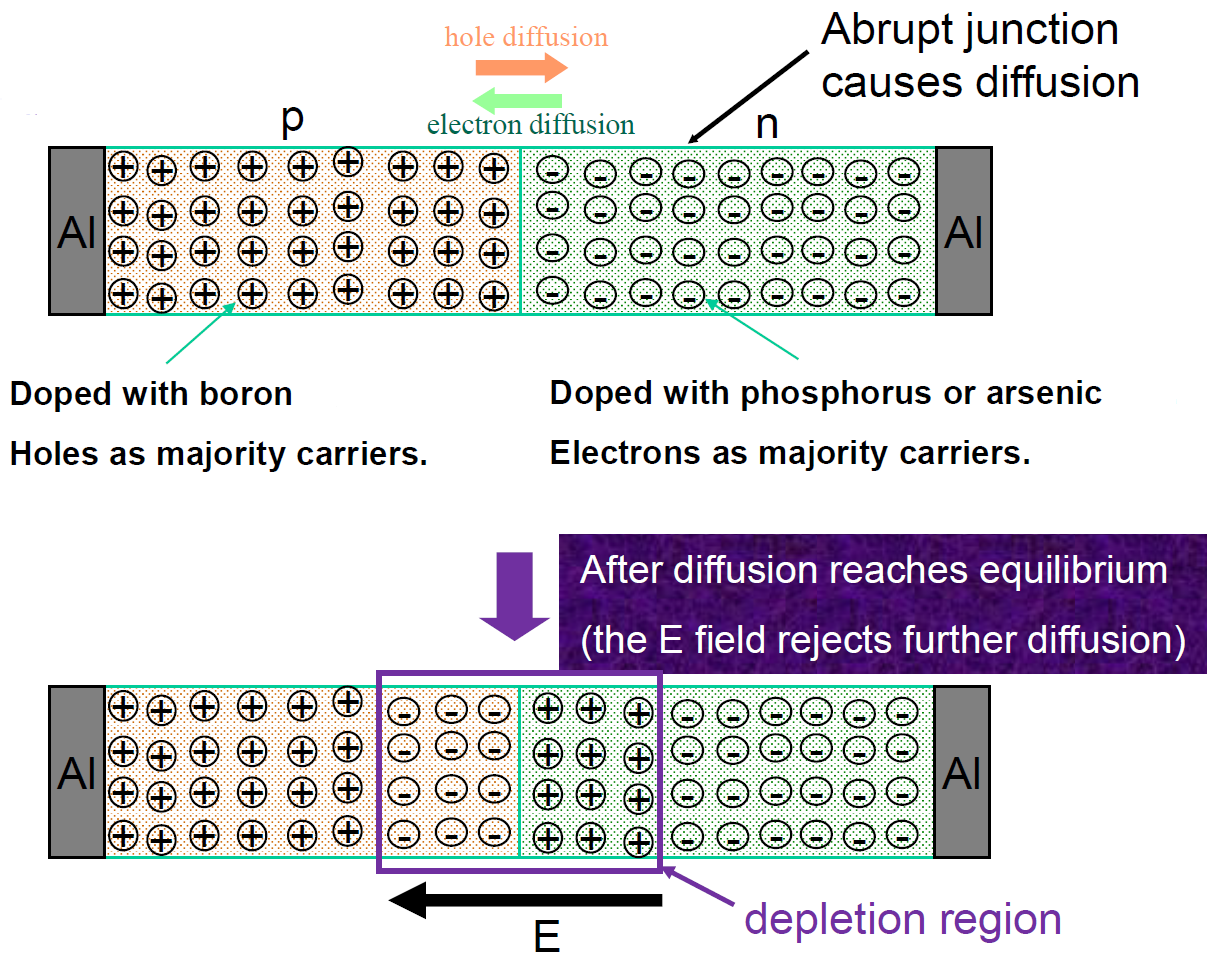
2.1 PN Junction
Diode on a Silicon
PN Junction and Depletion Zone
The abrupt gradient causes diffusion, causing the depletion zone. In the depletion zone, there will be a build-in field, causing drift.
The build-in field has a potential:
where is the thermal voltage,
are separately the accepter concentration and donor concentration.
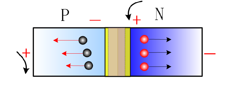
2.2 Bias
Forward Bias:
External field overcomes build-in field, large forward current (diffusion)
Depletion width decreases
Reverse Bias:
Extremely small reverse current (drift)
Depletion width increases (external & build-in same direction)
2.3 Current
2.4 Capacitance
PN Junction Capacitance
There’re charge on the sides of depletion zone, forming a parallel capacitance.
where is the cross-sectional area.
For abrupt junction, ;
and for linear junction, .
3. MOSFET-Static
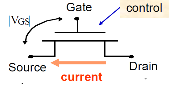
In a Metal-Oxide-Semiconductor (MOS) structure, the basic principle of conduction relies on an electric field controlling a channel. When a voltage is applied to the gate terminal, it creates an electric field that penetrates through the insulating oxide layer and into the semiconductor substrate. This field attracts or repels charge carriers (electrons or holes) in the semiconductor, forming a conductive channel just below the oxide.
For an N-channel MOS transistor, a positive gate voltage attracts minority carriers (electrons) to the surface of the p-type silicon, creating a thin n-type inversion layer. This layer acts as a channel that connects the source and drain regions, allowing current to flow when a voltage is applied between them. The size and conductivity of this channel are directly controlled by the gate voltage, enabling the device to function as a switch or an amplifier.
3.1 Concepts:
Source and drain are completely symmetric in fabrication. The only difference is the voltage.
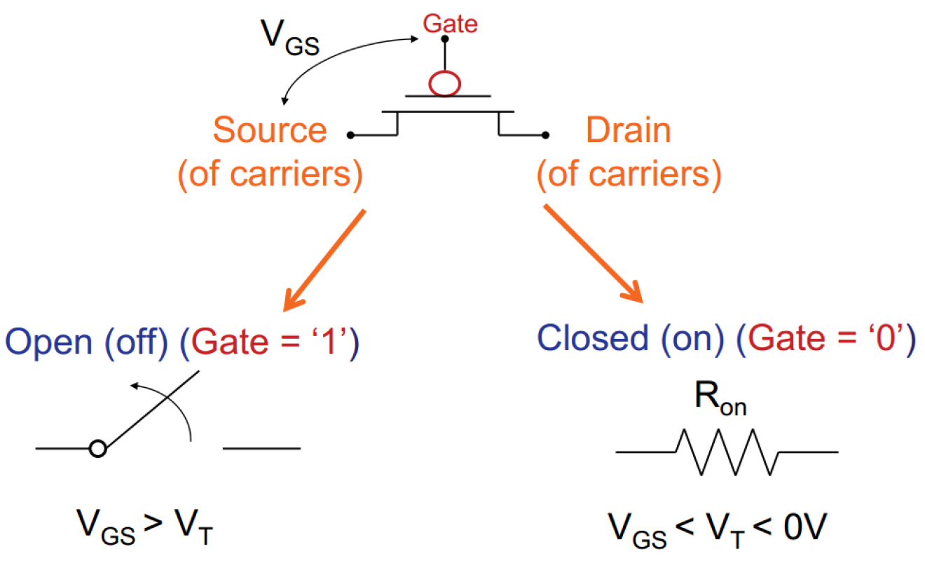
NMOS: Low voltage for source, high for drain
PMOS: High voltage for source, low for drain
3.2 Parameters
(length): Length of the (transistor) channel.
The minimum channel length is the most critical physical parameter
that characterizes the advancement of a CMOS technology.
(width): The (transistor) channel width.
Minimum width is fixed by the technology.
The parameter that the circuit designers decide
— Adjusted to tune the driving strength of a transistor
Theoretically, no limit for maximum.
3.3 VTC
NMOS VTC
PMOS VTC
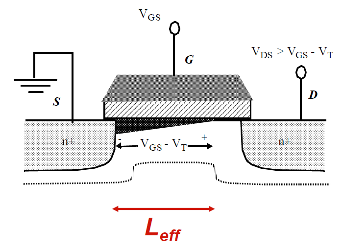
Take NMOS for example:
Building on the principles of MOS transistor operation, the device can operate in three distinct regions—cutoff, linear, and saturation—
based on the applied gate () and drain-source () voltages. These regions determine the transistor's function as a switch or an amplifier.
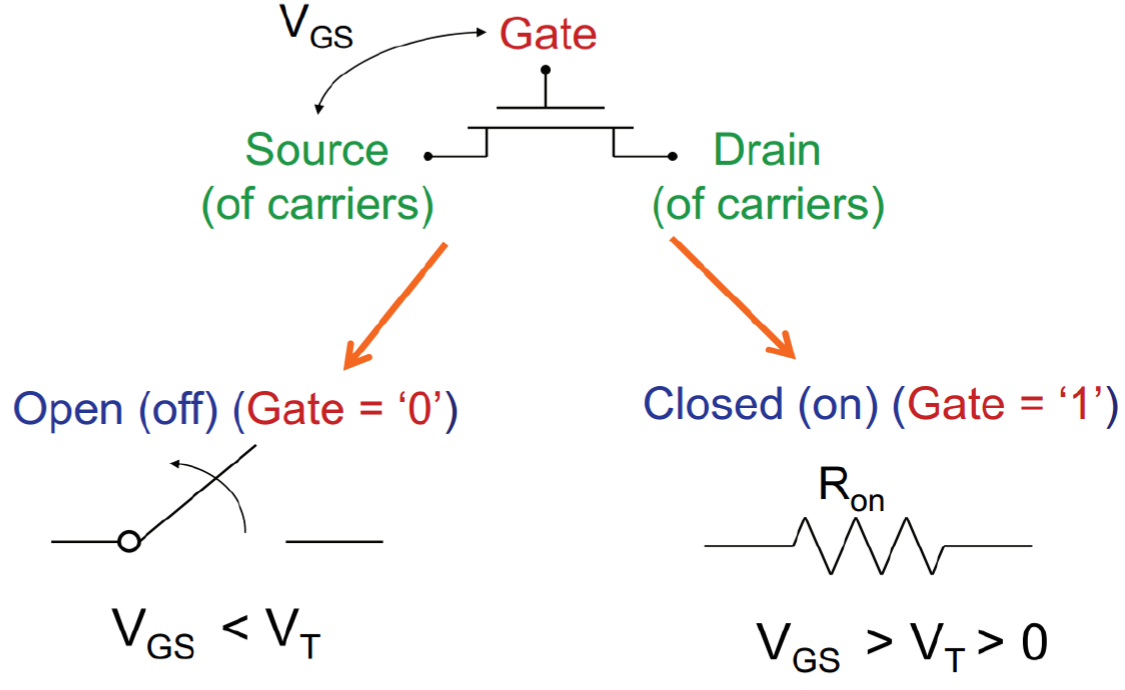
Cutoff Region
The transistor is in the cutoff region when the gate voltage () is less than the threshold voltage ().
In this state, the electric field from the gate isn't strong enough to attract enough minority carriers (e.g., electrons for an n-channel device) to form a conductive channel at the silicon surface. Without this channel, the source and drain terminals are effectively isolated. As a result, no drain current () can flow, regardless of the voltage applied across the drain and source. The transistor acts like an open switch, blocking current flow.
Linear Region (or Triode Region)
The transistor operates in the linear region when is greater than and the drain-source voltage () is small.
The gate voltage is now high enough to form a complete, continuous channel between the source and drain. Because is small, the voltage drop along the channel is negligible, and the channel's thickness is relatively uniform. This makes the channel's resistance nearly constant. Consequently, the drain current () is approximately proportional to , behaving like a voltage-controlled resistor. The value of this resistance decreases as increases.
Saturation Region
The transistor enters the saturation region when is greater than and increases to a certain point.
As rises, the voltage at the drain end of the channel, which is equal to , decreases. When this voltage drops below the threshold voltage, the part of the channel near the drain terminal is "pinched off." The channel effectively disappears at this point, and the current flows through a high-field region to the drain.
Despite the pinch-off, the current does not stop. Instead, it becomes nearly constant because the current is primarily determined by the carrier density at the entrance of the channel. In this region, the MOS transistor acts as a voltage-controlled constant current source, which is the key operational mode for amplifier circuits.
Mathemathecally
Cut-off: , no current
Linear: ,
and are approximately linear.
: Electron mobility, which describes how easily electrons move through the semiconductor channel. It is measured in .
: Gate oxide capacitance per unit area, which depends on the thickness and material of the gate oxide layer. It is measured in or .
Saturation: ,
almost remains constant.
3.4 Channel-Length Modulation
When MOSFET reaches saturation,
part of the channel will be pinched-off,
causing a shrink of the effective channel length as increase.
Sketch of Pinch-off
Given this effect,
the formula should be repaired:
The is a empirical parameter,
reflecting the effect of channel modulation.
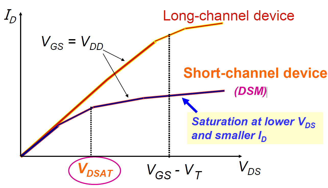
3.5 Velocity Saturation
When the electrical field along the channel reaches a critical value, the carrier velocity tends to saturate due to scattering effects (collisions suffered by the carriers).
Since the carrier velocity has reaches a constant,
the current will no longer increase as increases.
This phenomenon is called velocity saturation.
Such effect only matters in short channel devices.
For long channel ones, is large,
even if is large,
the electrical field is still small,
which is not enough to saturate the velocity.
But in short channel ones,
is small.
It's easy to form a large electrical field.
Hence, velocity saturation is important in short channel devices.
The essense of velocity saturation is electrical field.
Short channel MOSFET enters saturation at before reaches ,
experiencing an extended saturation region.
Then the amount of current is reduced for a given control voltage.
Effect of Velocity Saturation on Short Channel Devices
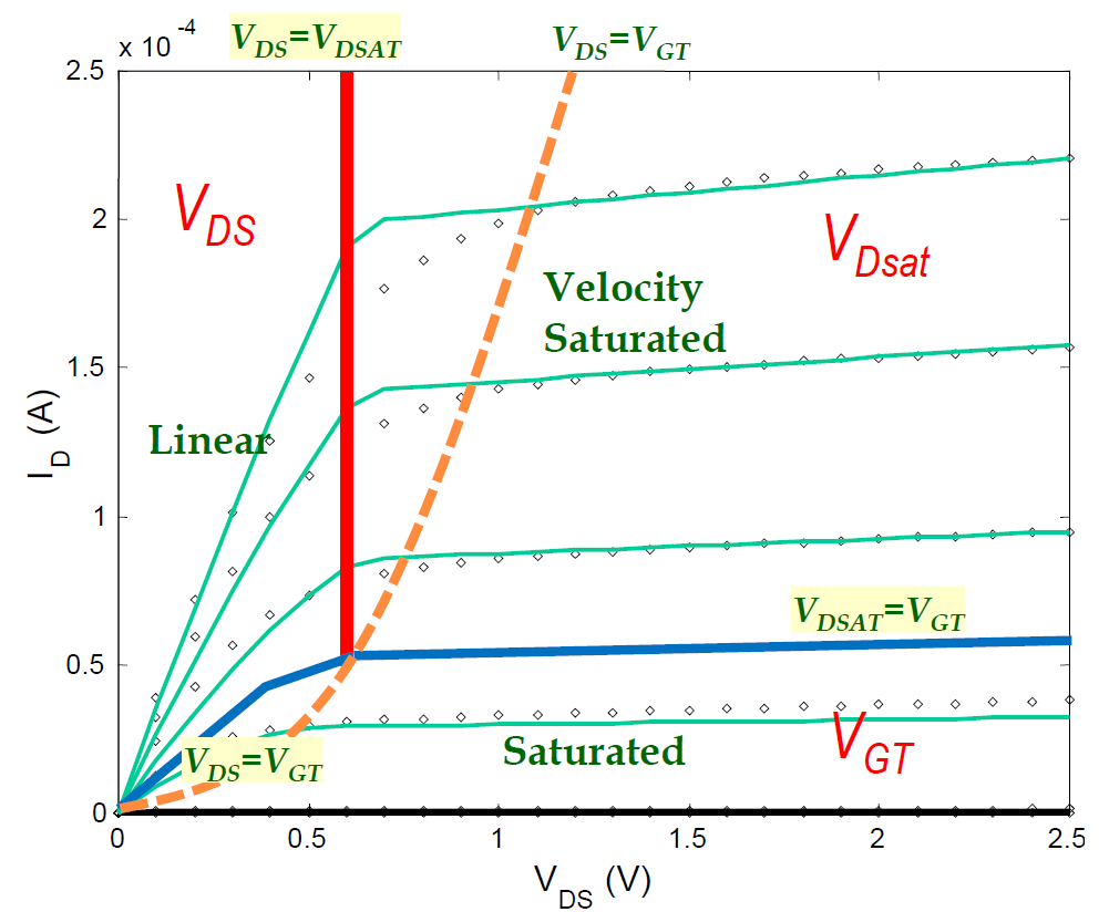
Given velocity saturation and other short-channel effects, we need a unified current model that works seamlessly across all operating regions. The key insight is to recognize that the current is always limited by the smallest “voltage headroom” available.
We define as the gate overdrive voltage, and introduce a unified model:
where
This model elegantly handles all three regions:
Cutoff: When , , and
Linear region: When is the smallest, , recovering the linear region equation
Saturation: When or is the smallest, becomes constant, giving saturation behavior
The parameter represents the drain saturation voltage considering velocity saturation:
where is the critical electric field for velocity saturation.
This unified approach eliminates discontinuities at region boundaries, making circuit simulation more robust and accurate.
3.6 Equivalent Resistance
In digital circuit analysis, we often need to estimate the charging/discharging time of capacitive loads. For this purpose, we define an equivalent resistance that approximates the nonlinear I-V behavior of a MOSFET with a single resistor value.
The equivalent resistance is defined as the average resistance during a output transition from to (for charging) or from to (for discharging). For a capacitor being charged through a PMOS transistor:
where , and is the drain current when the output voltage is .
In saturation region (considering channel-length modulation), the current is approximately:
Substituting and integrating from to :
For small , we can expand using Taylor series:
This equivalent resistance allows us to estimate delay as , greatly simplifying digital timing analysis.
3.7 Source and Drain
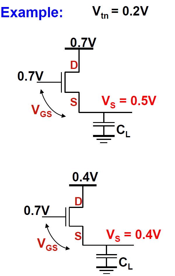
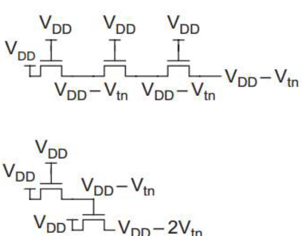
Take NMOS for example:
Example for Source Voltage
In the first figure,
once the gate voltage rised to ,
,
NMOS is turned-on.
S is charged by D.
But with time going,
rised.
Can it reach ?
If ,
,
the NMOS will be cut-off.
So to make NMOS keep turning on,
has a maximum value of .
Then in the second figure,
D still charged S.
But since current is from D to S,
with the resistance of ,
it's obvious that .
Meanwhile,
even at ,
the NMOS is still on,
so is reachable.
To recap,
the two cases can be joined into one equation:
4. MOSFET-Dynamic
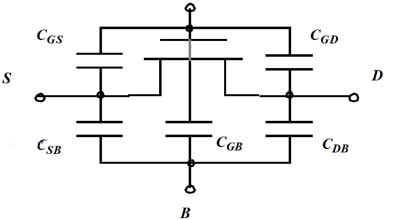
4.1 Capacitance Components
There are three sources of capacitance in a MOSFET.
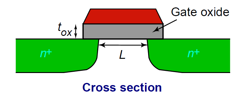
Overlap cap
Parasitic capacitance between the gate and source/drain caused by lateral diffusion extending beneath the oxide layer.
Gate-Source and Gate-Drain
: cap per unit area presented by gate oxide
: overlap cap per unit transistor width
: lateral diffusion length
: transistor width
: oxide permittivity
: oxide thick
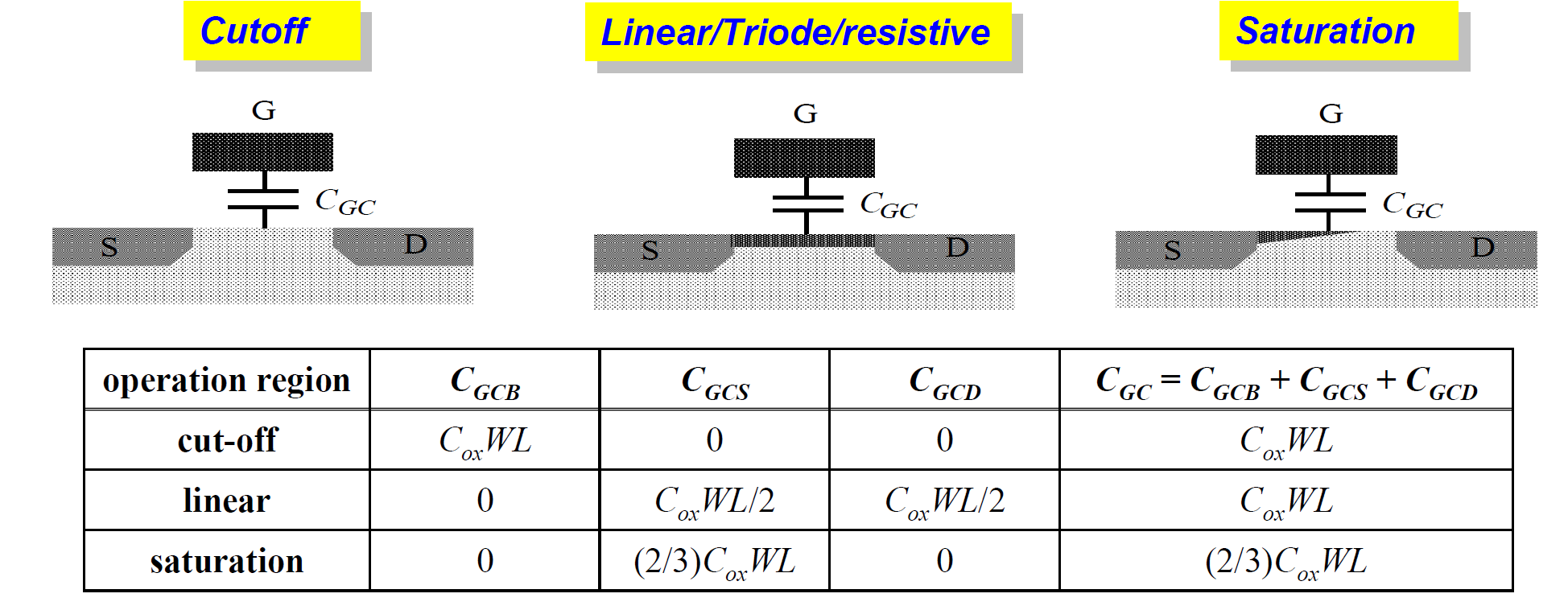
Gate-to-channel capacitances
Generates the channel charge required for transistor operation and depends on the transistor’s operating region.
Gate-Body, Gate-Source, Gate-Drain
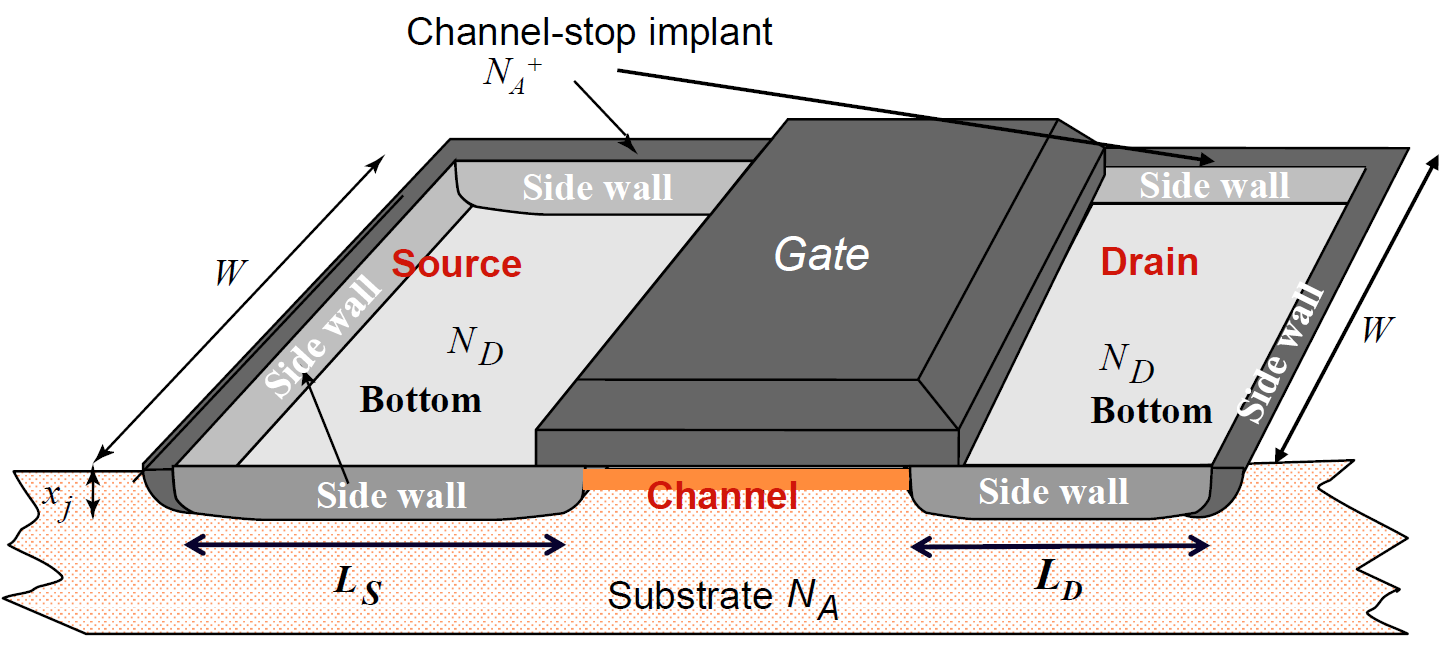
Junction cap: PN junction cap .
Junction / diffusion cap:
diffusion cap of source to body:
diffusion cap of drain to body:
: bottom-plate junction cap
: side-wall junction cap
: junction cap/unit area
: side-wall junction cap/unit perimeter
: area of bottom plate
: perimeter of side wall
: length of source region
: length of drain region
: transistor width
4.2 Body Effect
When the voltage of substrate changed, the threshold voltage will also change.
For NMOS
For PMOS
where is the substrate bias between source and body;
is threshold voltage for (determined by manufacturing).
is called the body effect coefficient,
expressing the impact of .
And
Positive for PMOS and negative for NMOS.
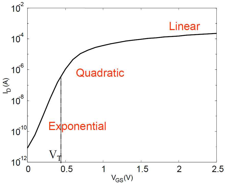
4.3 Sub-threshold Condition
Meaning .
In most digital ICs, sub-threshold current is not desirable (leakage),
which will cause heat and waste of power.
In sub-threshold region,
the slope of —— is
In this situation,
where
Leakage in sub-threshold region is the most impotant useless power source in modern IC.
5. Inverters
5.1 Static Behavior
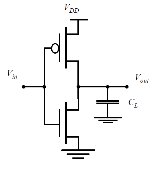
A CMOS inverter is composed with an NMOS and a PMOS.
Static CMOS inverter
When is low, NMOS is cut-off and PMOS is on.
The output is .
And conversely, high gives a low output.
Hence,
the output swing is between and ,
which results high noise margins.
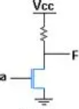
Meanwhile, the CMOS inverter is ratioless. This means the logic levels are independent from the external or interval configurations. Compare CMOS inverter to a single NMOS inverter with a pull-up resistor.
Single NMOS inverter
We know NMOS passes a strang 0, but a weak 1.
When the input is low,
the output is not ,
it depends on the resistor value and the equivalent resistance of NMOS
The high logic input depends on the configuration and parameter of the NMOS itself.
Such circuit is called ratioed logic.
CMOS inverter doesn't change logic level with parameters of NMOS and PMOS.
Moreover,
with the gate is alomst isolated with the bulk,
the input impedance is always large enough.
Output impedance depends on the equivalent resistance of MOS,
which is small enough.
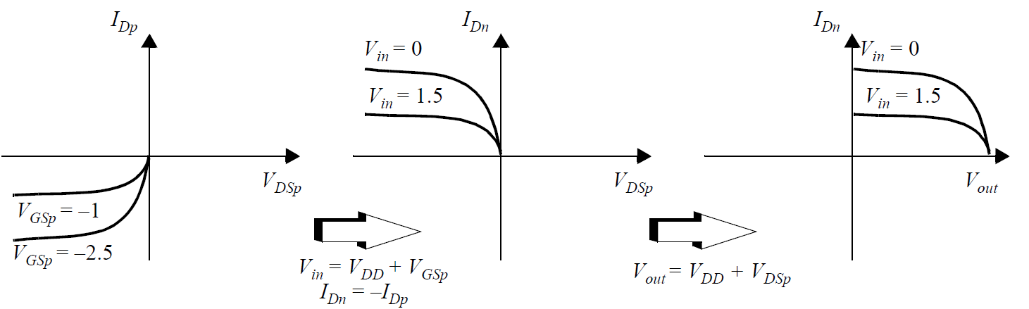
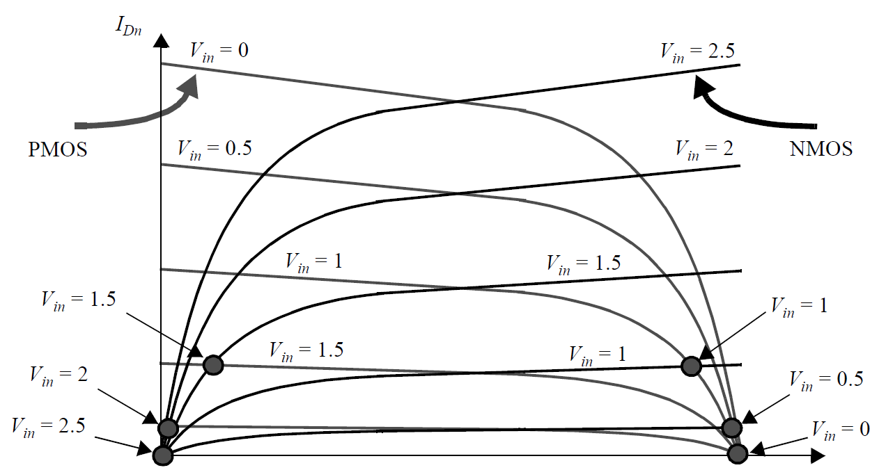
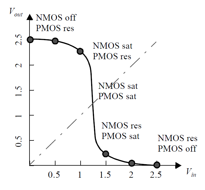
Now we deduce the VTC of CMOS inverter.
The basic idea to deduce is to plot the I-V curve of both NMOS and PMOS in the same coordinate,
find the crossing point under different ,
transform these points to - coordinate,
and then connect them together.
Then you'll get the VTC.
We start from the I-V curve, called load line.
Consider a CMOS inverter with no load.
By Kirchhoff's law and other characteristics, we have
The load-line curves of the PMOS device are obtained by a mirroring around the xaxis
and a horizontal shift over .
PMOS Load Line
Then draw NMOS load line. We get a figure
Cross Figure of PMOS and NMOS Load Line
Record and and plot,
we get the VTC
CMOS Inverter VTC
5.2 Robustness
There are some indices to evaluate CMOS inverter robustness.
Swithcing Threshold
The switching threshold is defined as value when .
In this region, PMOS and NMOS are both saturated since .
We can solve by equating the currents in saturation region.
with high voltage supply (velocity saturation) and channel-length modulation ignored:
Solving this equation
For large values of (compared to threshold and saturation voltages), the equation can be simplified:
The ratio compares the driving ability of PMOS and NMOS.
In general is desired to reach .
Hence, the most ideal case lies in that ,
meaning a complete symmetry between PMOS and NMOS.
Deviation from 1 will skew the VTC curve toward GND or VDD.
When the inverter is fabricated with long-channel process
or the supply voltage is low,
it may fail to reach velocity saturation.
In this case the position of in the equation will be replaced with .
Then
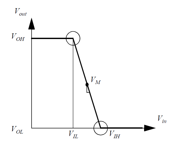
Noise Margins
In the VTC curve, noise margins and are defined by
Input voltage above can be regarded as a valid 1
and that below as a valid 0.
Input between the two values are regarded invalid,
represented by X and will be dropped.
Such a definition lies on the essence of gain.
Giving a DC input bias on the point of ,
then apply a small AC signal around this point.
At this point, with a slope of -1,
the amplitude of this AC signal will not change.
We say the inverter has a AC gain of -1 (negative for inverse phase) at this point.
For , before this point, we regard the small variation vanishes,
the output remains VDD;
After this point the variation will cause a collapse from VDD to GND
(vice versa for ).
To simplify the problem,
the VTC curve is simplified into three line segments.
The two points satisfying serve as inflection points. the boundary of the segment.
Simplified CMOS Inverter VTC
With this simplification,
the gain is obvious:
A more precise definitioin for noise margin is
Without simplification,
the gain should be calculated by the current formula
Differentiation and solving for yields
yields
Of course, for the gain, the larger, the better.
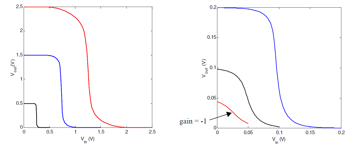
When the supply scales, also scales with it.
From the formula above,
the smaller , the stiffer the VTC is in the undefined region (between and ).
Hence,
when the supply voltage decreases,
the gain will increase.
This tells us that we'd better apply a low supply in high precision cases.
However, when the supply is too low,
both MOS's cannot be completely cut-off and leakage cannot be ignored.
In this case, the gain will decrease with supply decreasing further.
5.3 Dynamic Behavior
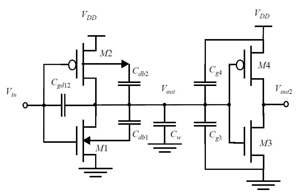
Capacitance
Dynamic behavior focuses on the propagation delay of the transient process. Such delay is caused by parasitic capacitance.
Consider a cascade of two inverters, one as driver and another as load.
Inverter in cascade with parasitic capacitance
The parasitic capacitances are composed by:
Gate-Drain Capacitance,
Diffusion Capacitance (Drain-Bulk),
Load Gate-Source,
Wire Parasitic,
All the cap's above will be equivalent to a total load cap to simplify.
This cap is connected between the output end and GND.
To deduce this cap,
all cap's must be equivalent to cap's connected between an end to GND.
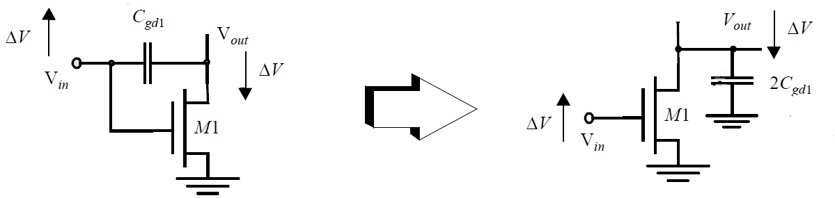
For , it can be directly equivalent by Miller's theorem.
Equivalence of GD Cap
For , it is mostly constructed by the reverse biased PN-junction.
Such cap is highly non-linear
Also, to simplify,
this cap can be equivalent to a linear mean cap.
In general
The wire cap depends on the wire length.
And the load gate cap (fanout) should be
Propagation Delay
Once lumped to ,
we can calculate the propagation delay.
Propagation delay is defined as
the time interval between input reaches 0.5VDD and
output reaches 0.5VDD.
The delay is caused by the charging/discharging to or from the cap.
Meanwhile the equivalent resistance (recall the formulas before),
This is a 1-order RC circuit.
Total propagation delay is
To optimize,
plug the MOS parameters in.
Take as example:
The method is obvious:
widen , shorten , lower , reduce , and so on.
Also, the propagation delay is related to the external load cap.
where is the delay without load,
called instrinc propagation delay.
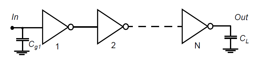
While sizing up an inverter reduces its delay, it also increases its input capacitance. Gate
sizing in an isolated fashion without taking into account its impact on the delay of the preceding
gates is a purely academic enterprise.
A more relevant problem is determining
the optimum sizing of a gate when embedded in a real environment.
A simple
chain of inverters is a good first case to study.
Inverter Chain
To determine the input loading effect, the
relationship between the input gate capacitance and the intrinsic output capacitance of
the inverter has to be established. Both are proportional to the gate sizing. Hence, the following
relationship holds, independent of gate sizing
the total delay is
is called effective fanout,
which is a ratio of total external load cap and input impedance of one inverter.
Such ratio is in fact the max number of inverters that an inverter can drive.
If the load exceeds ,
the output signal will fall in X region.
We can give the delay of th inverter stage
total
are unknown. To minimize the total delay,
differentiate these N-1 variables and equate
These equations get some constraints
This means different stages have the same effective fanout.
This fanout can be figured out, with and given
The minimum delay
In general, resistance of is not equal to . Hence, to match the resistance and get a equal delay for both edges (rising and falling), the PMOS is always widened to 3-3.5 times wider than PMOS. That means
The motivation to do this is to create a symmetric VTC.
But what's the most proper ratio?
COnsider two CMOS inverters in cascade,
the load cap is
When PMOS is widened with ratio ,
related parameters scale approximately the same way.
Cap's are also scaled with ratio .
Then the total cap
Plug into the propagation delay
Optimization wants to minimize the delay,
hence we take partial derivative to
When the wire cap can be neglected,
5.4 Power
Load cap is charged through PMOS and discharged through NMOS.
When charged, draws energy from supply,
part of them stored in and another part dissipated at PMOS resistance.
When discharged,
the stored energy is dissipated on NMOS resistance.
Suppose there is no direct path from VDD and GND
(PMOS and NMOS are not on simutaneously).
The total energy drawn from supply is
In charging process,
the energy stored in is
This is an amazing result. Only half of the energy drawn from supply is stored and the rest half is dissipated in PMOS. The efficiency is independent of PMOS size. In a complete process of rising and falling, energy from supply is equally dissipated in PMOS and NMOS, respectively. Hence, to optimize power, the only two ways are reducing load cap or supply voltage. In general, reducing supply is easier to apply and more effective, for supply has a quadratic effect on energy consumption.
With time going, the power is
where is the frequency of switching from 0 to 1.
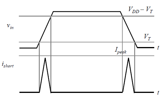
However, in actual designes the assumption of no direct path no longer hold for input signals with finite slope. When input is in X drop, the two MOS’s may be on simutaneously and form a direct current path between VDD and GND, which introduces extra dynamic power consumption:
This state can last for only a short time.
Hence the consumption in this period can be approximated as a triangle in I-t coordinate.
Both rising and falling edge have such a period,
so there must be two terms:
The average power consumption:
Timing of a Complete Switch Process
The both on state occurs when the input is between and
(Note that ),
Denote ,
then
where is the rising or falling time of the input.
is determined by the saturation current of both MOS's.
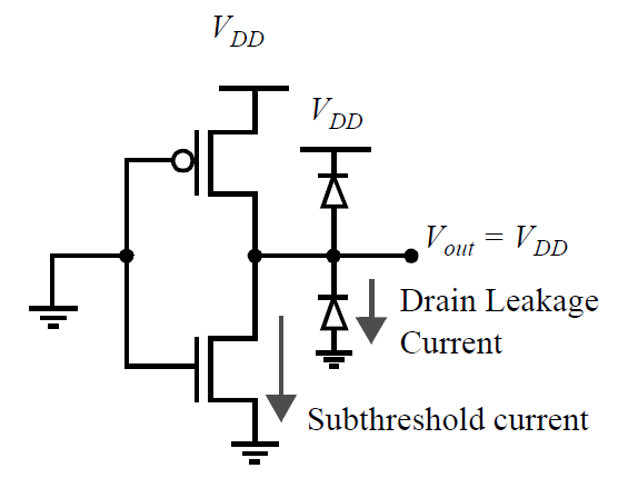
When the inverter is stable, ideal static current should be zero, hence the static power is zero. However, unfortunately there will be a leakage from supply rail to GND. Some carriers will leak through the reversed bias PN-junction between source and drain. In general this leakage is extremely small and can be ignored. The static consumption is therefore
Leakage from Source to Drain
This leakage is caused by thermally generated carriers, and the number of such carriers increase with rising of temperature exponentially.
To sum up, the total power consumption of an inverter should be
The three terms are in descending order of importance.
Now introduce some measure for abilities of a logic gate.
Power-delay product (PDP)
PDP has a unit of Joule (energy),
measuring the maximum average energy consumed per switching.
Under maximum switching frequency ,
we find
Energy-delay product (EDP)
EDP is an index for trade-off between delay and power consumption.
Increasing will reduce delay, but harm the consumption.
Since
(ignore channel-length modulation),
delay and supply are negatively correlated,
approximately inverse.
while consumption is quadratically, positively correlated with supply.
EDP is a measure to balance the two indices.
In actual designs,
we try to minimize EDP,
to get a totally best performance.
Simplify the above
where .
Combine it with PDP,
The best point of supply satisfies
References:
[1] J. M. Rabaey, A. Chandrakasan, and B. Nikolić, Digital Integrated Circuits: A Design Perspective, 2nd ed. Upper Saddle River, NJ: Pearson Education, 2003.