Analog Integrated Circuits

Copyright Notice:
This article is licensed under CC BY-NC-SA 4.0.
Licensing Info:
- Title: Analog Integrated Circuits
- Author: EleCannonic
- Link: https://elecannonic.github.io/categories/electronics/analog_integrate/
Commercial use of this content is strictly prohibited. For more details on licensing policy, please visit the About page.
1. MOSFET
1.1 MOSFET in CMOS
A typical fabrication of NMOS is shown in the figure below.
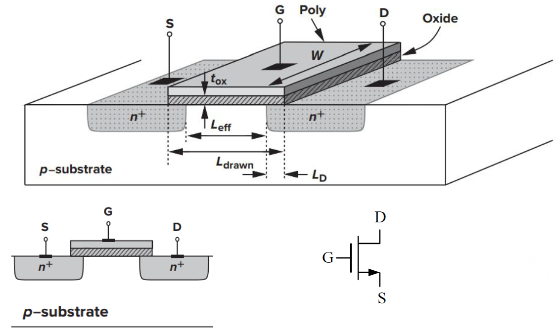
The NMOS is grown on a p-substrate,
which contains
First discuss cases of
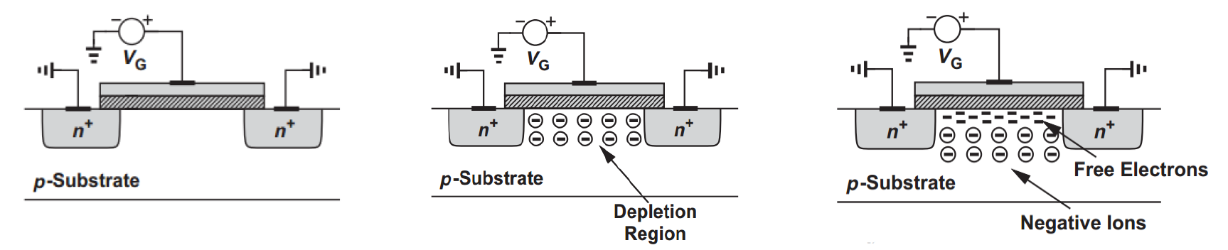
Obviously nothing happens in the NMOS, no electric field. NMOS is cut-off and at equilibrium.
Positive voltage at gate produces a vertical
Some of the minority
The attracted
However, the
It’s not enough to attract adequate
hence there’s still no free
Now
The MOSFET is on.
On the surface of p-sub,
the
the remaining
forming a conductive channel.
The threshold voltage of
The threshold voltage is related with doping, material and process. Generally,
PMOS has one more step than NMOS in fabrication. There’s an n-well on the p-sub, then 2 p-semiconductor S and D.
1.2. Large Signal Behavior.
Cut-off:
. . Weak Inversion / Sub-threshold Region.
, but .
With depletion region, there’s no drift current, only diffusion current.
Diffusion current depends on the concentration density of
The gradient satisfies
It can be deduced.
where
At room temp.
- Triode Region.
, .
We can define overdrive voltage
as how much
We apply a voltage at D, generating a
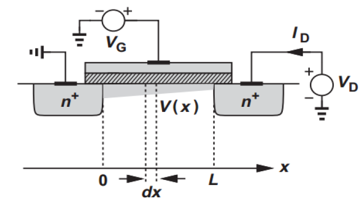
The charge at
where
Integrate over entire channel length
Hence
- Saturation Region
If
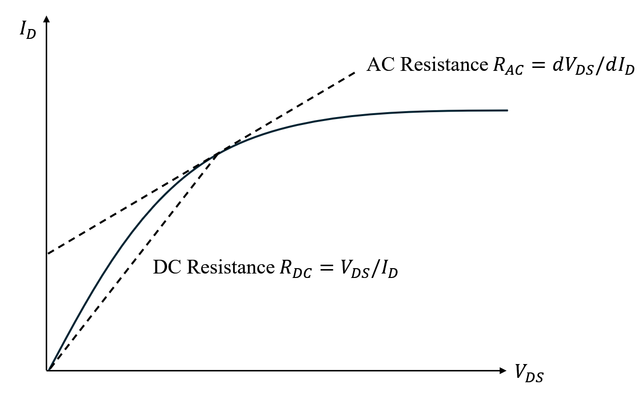
1.3 Channel Length Modulation.
Considering pinch-off in saturation region.
Since pinched-off channel is shorter relative to lower device, hence the longer the channel, the weaker channel length modulation is.
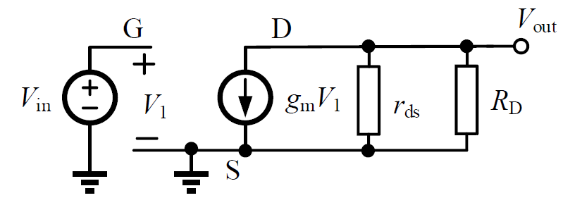
1.4 Small Signal Analysis
With a specific DC bias (large signal),
the small signal analysis evaluates how much effect a small variation based on DC bias causes.
The MOSFET small signal equivalent circuit is shown below.
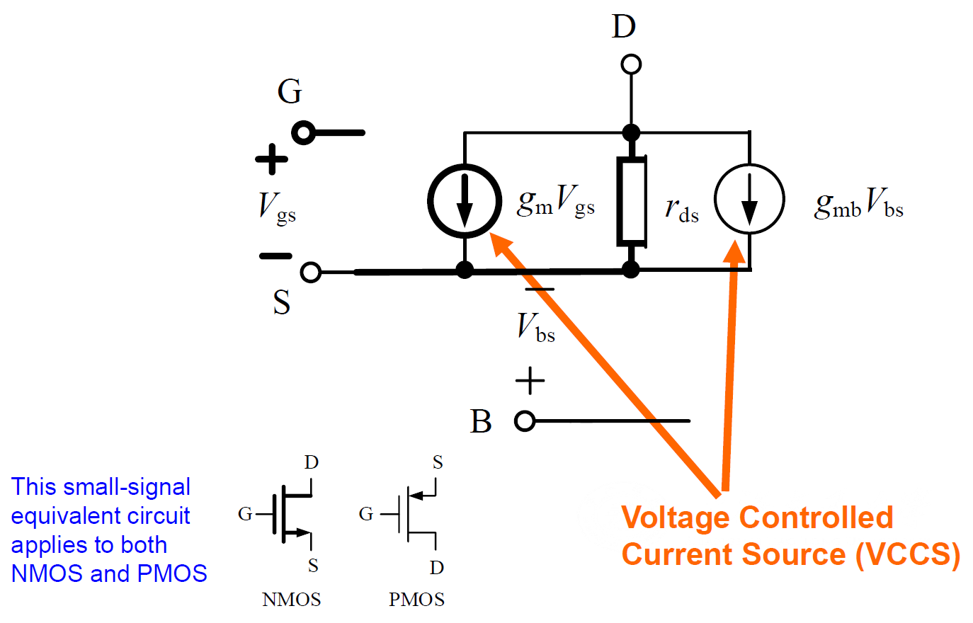
Under DC bias
Approximate
the three terms represents three current branches. Hence there must be three branches between
Plug these parameters in
In saturation
So
Note that
Since bulk/substrate is always connected to the GND (NMOS) or VDD (PMOS),
to simplify problems, we regard
so
But when the drain (NMOS) or source (PMOS) is not connected to GND or VDD,
this term must be taken into consideration.
Also, the impedances
We hope to have large
So we have to balance the two parameters. Define intrinsic gain
Also
We know the small signal voltages are approximation of differential, hence in small signal model, we only take variation into consideration. All constant voltages (DC flatten) in large signal model are considered as AC-GND,
including GND, VDD, bias, and so on.
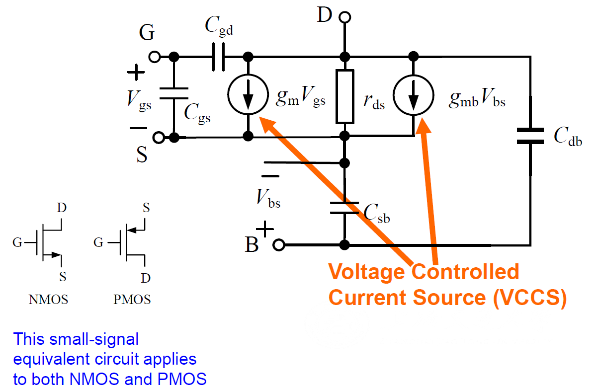
1.5 Complete MOSFET Small Signal Model
With high freq. input, the capacitance between different parts can no longer be ignored.
2. Single-Stage Amplifiers
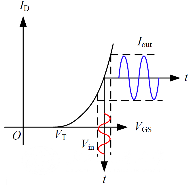
2.1 Insight of Amplification
Recall the intrinsic gain of MOSFET small signal model. For more amplification circuit, it can be expanded
So why MOSFET can amplify? For MOSFET.
The resistance of large and small signals are separated. The large signal resistance must be finite, while small signal resistance may be infinite (in saturation, approximately). So the separation of DC and AC resistance is also an important reason to amplify.
An opposite example is resistors. Also follow the two steps, voltage to current, current to voltage. For resistors
They’re not independent, and
No amplification.
2.2 Amplifier Concepts
The voltage gain:
The current gain:
The power gain:
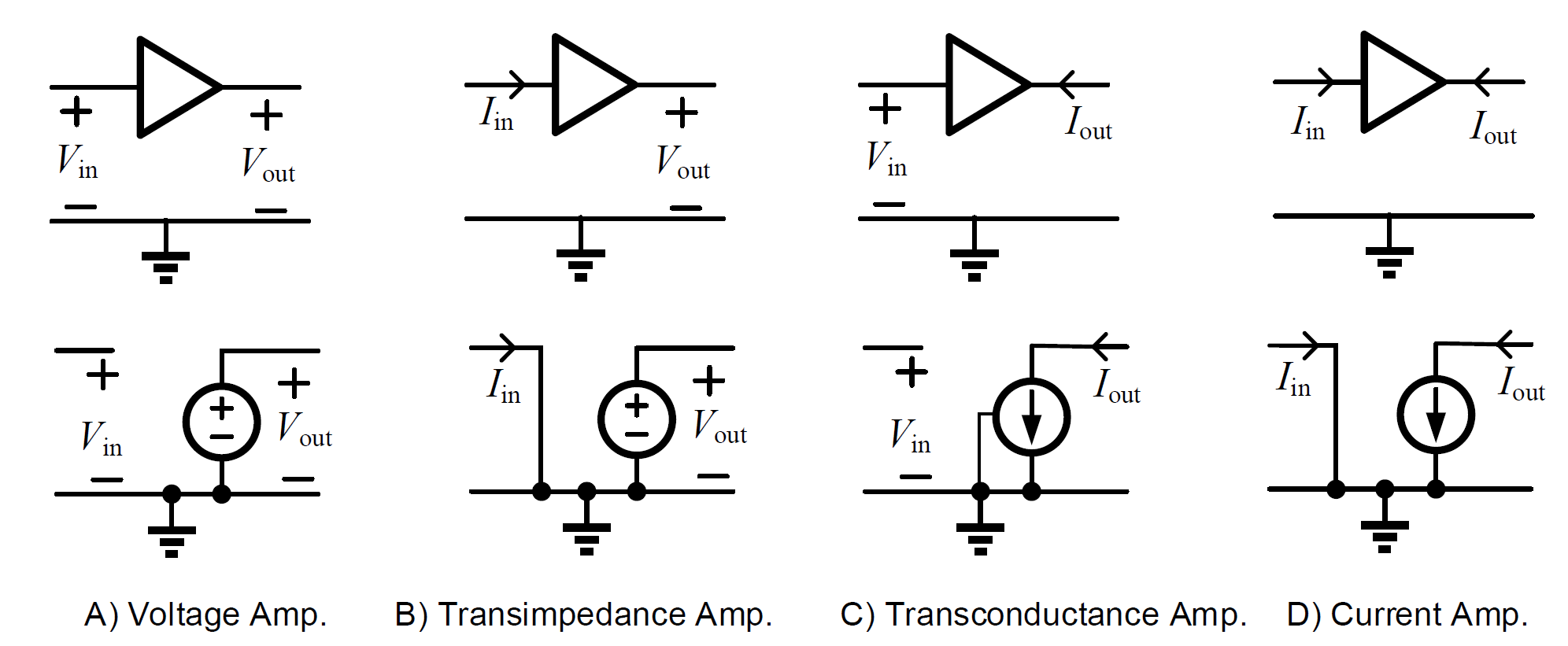
There are 4 types of amplifiers.
2.3 Three configurations of MOSFET Single-Stage Amplifier.
There are 3 configurations:
- Common Source: input G, output D
- Common Gate: input S, output D
- Common Drain: input G, output S
Note that for all configurations the MOSFET should always be in saturation region.
A MOSFET is a 4-port device. Ignore the bulk, we can list the impedance of the remaining 3 ports (relative to AC-GND)
- Gate:
, , control current source. - Source:
(low impedance), , control current source. - Drain:
(high impedance), , can’t control current source.
Originally there should be 6 types of configuration:
- G → S
- G → D
- S → G
- S → D
- D → G
- D → S
Now we analyze each of them
can control, can output, able to amplify. can control, can output, able to amplify. can control, , unable to amplify. can control, , able. can't control, unable. can't control, unable.
If the current source cannot work, the MOSFET become a resistor.
We have known a resistor can’t be used for amplification,
so the current source must be actively controlled..
Hence there’re only 3 configuration remaining, available for amplifier.
Check the small model, ( impedance relative to
According to Thevenin’s theorem, the G→S configuration exhibits large input impedance and small output impedance. This results in higher voltage division at the input terminal and greater voltage transfer to the load. Therefore, G→S is suitable for voltage input and voltage output applications.
Similarly, G→D configuration is appropriate for voltage input and current output operation, while S→D configuration works well for current input and current output scenarios.
2.4 Common-Source Amplifier
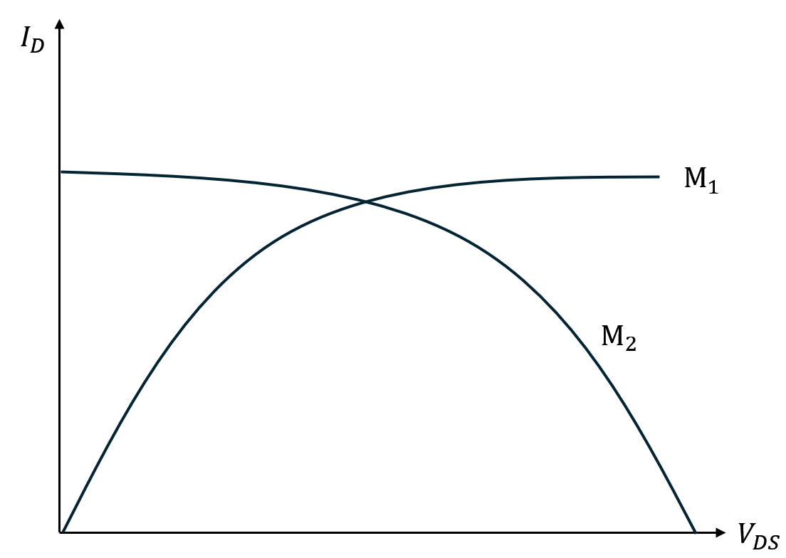
The input is applied to gate, output is taken from D. The source is the common reference point.
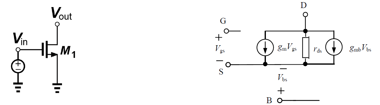
- DC Analysis.
At
Current on
Increase
When
The slope reflects the intrinsic gain.
From the figure, the slope is negative, hence
- AC Analysis
Now it comes to the small signal (AC). Replace the DC voltage sources with GND.
By KCL:
It gives
Also, we can also say
In practice, we assume
To raise the gain, we can raise
Plug in
Hence to raise
But trade off is necessary here. Such optimization will bring larger device size and capacitance, causing lower speed.
If the MOSFET works in the triode region (
It has no amplification function.
Back to the saturation, since
- MOS to replace
.
This MOS is configured in the triode region.
In process some parameters may drift. By using a PMOS to replace
However such cancellation is not stable. So there’s another method.
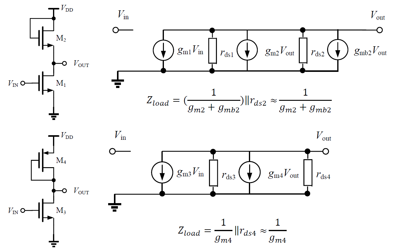
The MOS to replace
Since
Gain
If the two MOSFETs are all NMOS, the parameter drift in process is almost the same, so they cancel better and are more precise. In fact the second NMOS serves as a DC current source. Then in AC analysis,
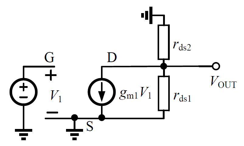
However, for the second MOS,
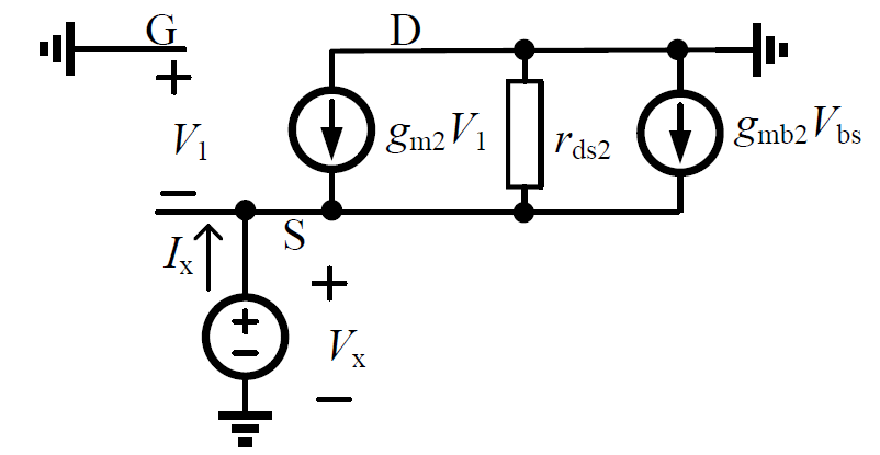
The resistance
To cancel bulk bias, use PMOS to replace NMOS
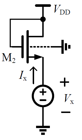
Bulk of PMOS is connected to VDD, which is the same as source.
Hence the bulk bias is cancelled.
But this circuit has some fatal problems:
- Only half of the MOSFETs are used to amplify, causing a waste of current
- It is sensitive to process corner (asymmetry between NMOS and PMOS)
- It can only deal with a very small range of signal.
The total DC model can be plotted.
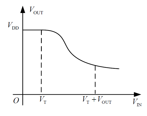
2.5 CMOS Inverter
To reduce waste, we need to place the crossing point into two saturation points. However, forcing two lines almost parallel is very difficult. In most case at least one MOSFET works in triode region.
The circuit must be changed. We connect
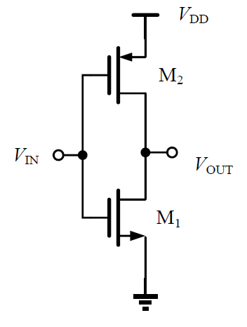
This is two amplifiers. When NMOS amplifies, PMOS serves as its load and vice versa.
In fact this is a digital inverter.
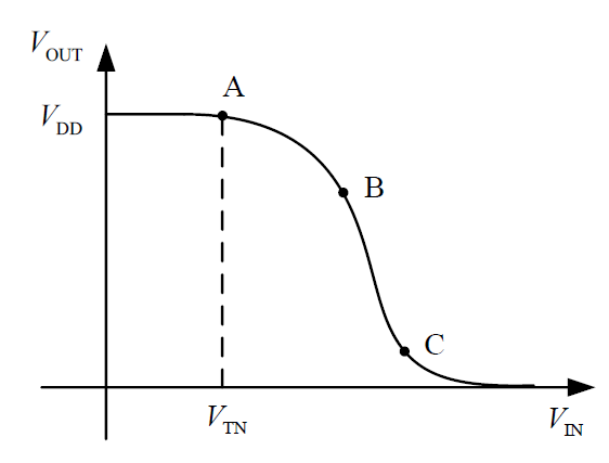
Its DC characteristic is shown below.
For AC model,
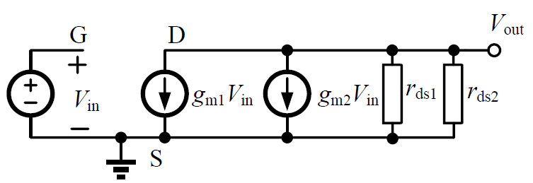
The transconductance is
With
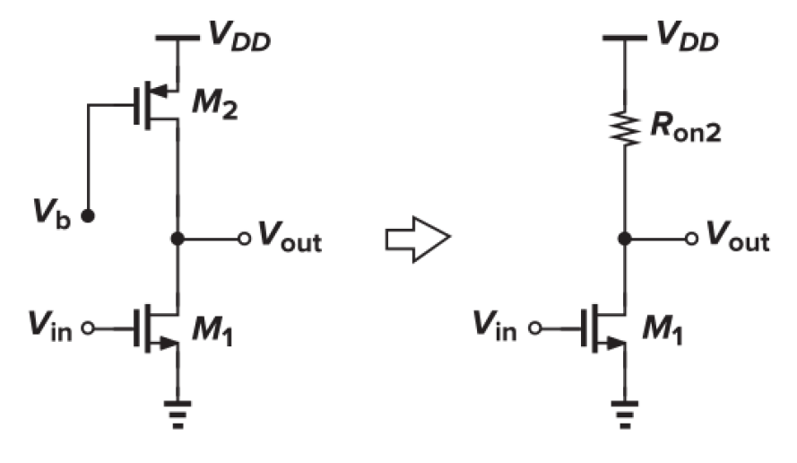
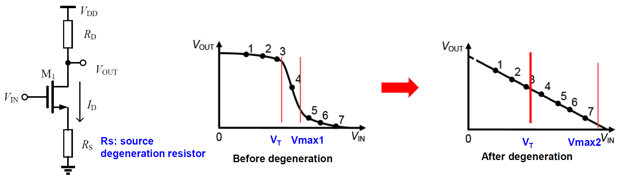
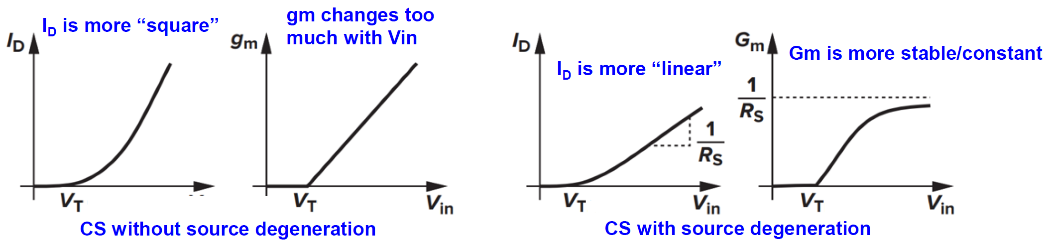
2.6 Source Degeneration
At this time the problem of current waste is solved. But the
Connect D with GND, by KCL:
Eliminate
The effective transconductance:
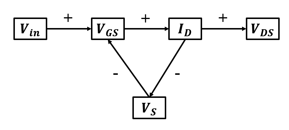
The key to widen the range of input voltage is negative feedback. Without the source resistor, when the input voltage increases, the gate-source voltage increases, leading to a rise in drain current and a drop in drain-source voltage. This makes it easy for the transistor to enter the triode region.
However, with the source resistor present, when the drain current increases, the source voltage also increases. This compensates for the variation in gate-source voltage, preventing significant changes in gate-source voltage. As a result, the drain current remains relatively stable, and the drain-source voltage also maintains stability, keeping the MOSFET in the saturation region.
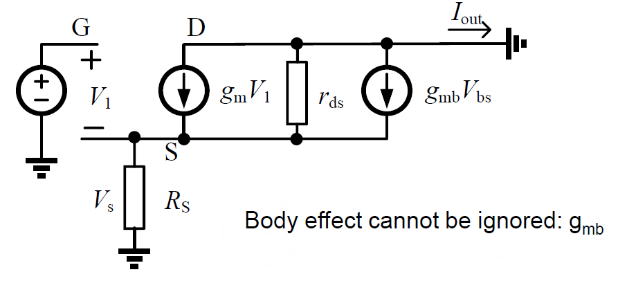
Now it comes to impedance. Apply voltage source
Eliminate
Finally we have the gain of common source with source degeneration:
It remains constant! Source degeneration only changes the range of double saturation.
Source degeneration has other advantages. In original amplifier:
The circuit parameter is influenced by the input signal, generating new frequency components, introducing non-linear distortion, but with source degeneration:
It is independent of the input (in saturation).
References:
[1] B. Razavi, Design of Analog CMOS Integrated Circuits, 2nd ed. New York, NY, USA: McGraw-Hill Education, 2017.