Analog Integrated Circuits

Copyright Notice:
This article is licensed under CC BY-NC-SA 4.0.
Licensing Info:
- Title: Analog Integrated Circuits
- Author: EleCannonic
- Link: https://elecannonic.com/categories/electronics/analog_integrate/
Commercial use of this content is strictly prohibited. For more details on licensing policy, please visit the About page.
1. MOS Devices
1.1 General Considerations
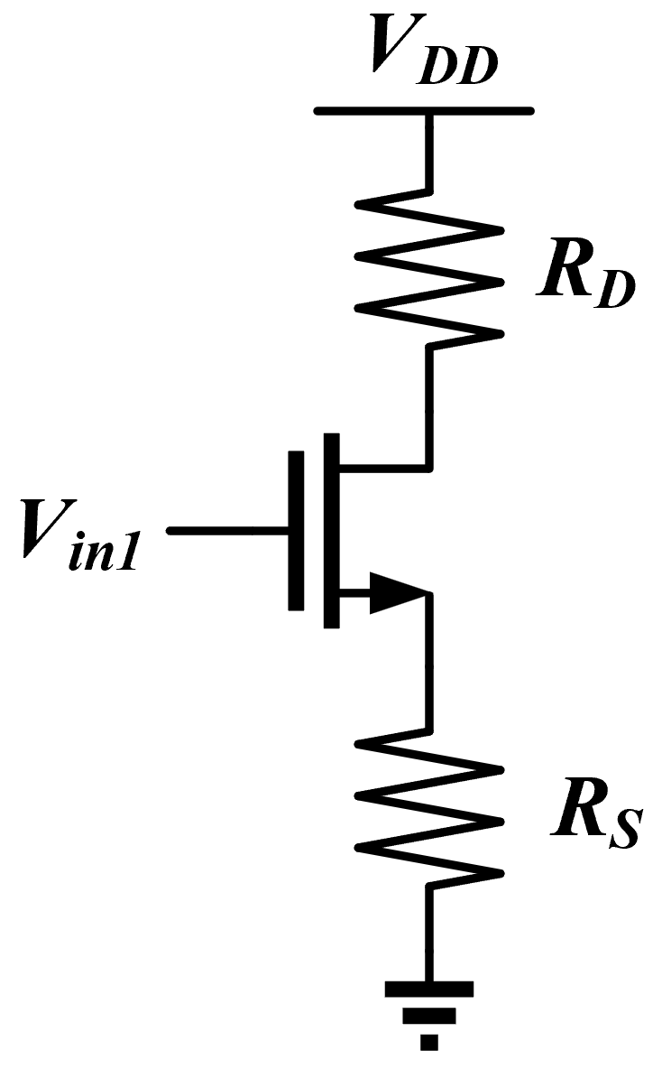
A MOSFET comprises a gate (polysilicon), a substrate (P/N semiconductor), a source (N/P semiconductor) and a drain (N/P semiconductor). The source and drain are interchangeable due to their symmetry during fabrication. There are two types of MOSFET: If the substrate is made of a P-type semiconductor (and the source and drain are made of an N-type semiconductor), it is an NMOS device; conversely, if the substrate is made of an N-type semiconductor (and the source and drain are made of a P-type semiconductor), it is a PMOS device. A typical NMOS structure is shown below:
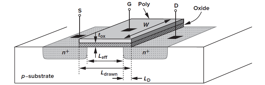
The lateral dimension of the gate along the source-drain path is called the length,
In long channel processes, the diffusion length can be ignored so we approximate
Since the source and drain are symmetric, we call the carrier provider as the source. For example, in an NMOS, terminal with the lower voltage is cthe source because it provides electrons to establish the current.
In reality MOSFET is a 4-terminal device. The last terminal is the substrate. In typical MOS operation, the S/D junction must be reverse biased, thus we assume the global p-substrate is connected to the most negative supply.
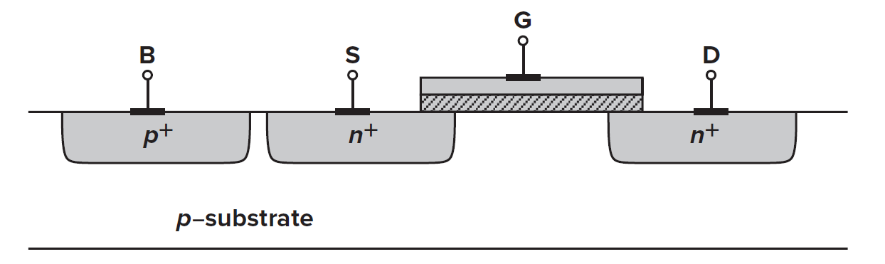
But for PMOS the substrate is independent because it needs a n-well on the p-substrate.
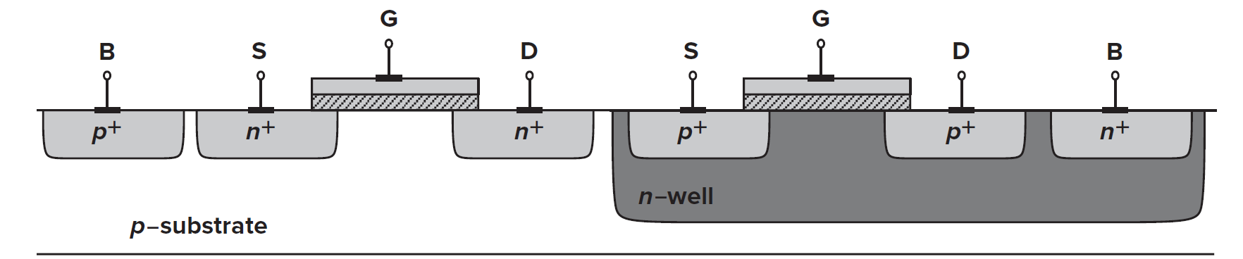
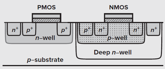
And in some modern processes, we make a deep n-well first and make another p-well inside to fabricate a NMOS to decouple the substrate with other devices.
Generally, if not specially designated, p-substrate in NMOS is connected to the lowest supply (negative supply or GND) and n-well in PMOS is connected to the highest positive supply. Then in the symbol we neglect substrate terminal by default.
1.2 MOS I/V Characteristics
MOSFET has a characteristic of switch. Now we analyze it.
Consider an NMOS connected to external voltages, with source connected to GND. When the gate voltage
In semi-conductor physics, it can be proved that
where
In fabrication, the threshold volatge will be adjusted by modifying the concentration of dopants to meet differernt requirements.
The source is not necessarily to be connected to GND. Thus, the
For PMOS, its switching characteristics are similar to those of NMOS, but in the opposite direction. It turns on when
In order to obtain the relationship between the drain current of a MOSFET and its terminal voltages, we make two observations.
First, consider a semiconductor bar carrying a current
Consider a NMOS whose source and drain are both connected to GND, indicating
The extra voltage
But when the drain voltage is greater than 0, the local difference between gate and the channel varies from
Where the
The negative number comes from the electron.
In semi-conductors,
Thus
The boundary condition indicates
Since
This is the I-V characteristic when
The peak current is
We call
In triode region the V-I curve is approximately a line. So we can estimate the equivalent resistance if
But what happens if
Note that in the figure the channel width represents the charge density instead of geometric width. In saturation region, the current is almost the same as that at
If
To recap:
- Cut-off Region:
, - Triode Region:
, , - Saturation Region:
, ,
Similarly, for PMOS, the current formula is
The negative symbol appears because the current direction is opposite to that of NMOS. In NMOS
1.3 MOS Transconductance
From sections above, we can see a MOSFET controls
$$
g_m = \dfrac{\partial I_D}{\partial V_{GS}}\bigg|{V{DS} \text{const}} = \mu_n C_{ox} \dfrac{W}{L}(V_{GS} - V_{TH})
$$
Each expression is useful.
For example, in practice
1.4 Second-Order Effects
- Body Effect
In the analysis before, we tacitly assumed that the bulk and the source of the transistor were tied to ground. What happens if the bulk voltage of an NMOS drops below the source voltage? In fact the MOS still works properly but some characteristics changes. Recall the threshold voltage analysis before. If the substrate voltage changes, as
It can be proven
Where
Since
- Channel-Length Modulation
Recall the current in saturation, we replace
This effect influences more in short channel processes. In long channel processes, it is usually neglected.
- Subthreshold Conduction
In reality the device does not turn on or off abruptly at
where
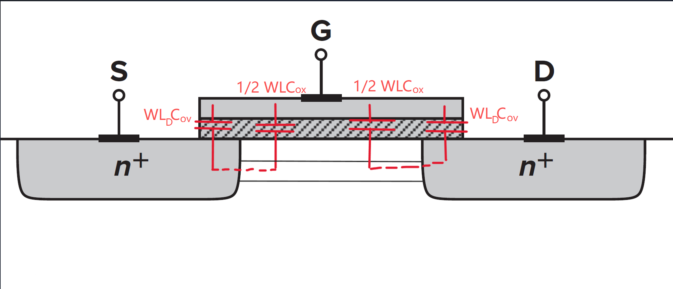
1.5 MOS Device Capacitances
Note: We will denote “capacitance” as “cap.” to simplify the decription.
We know there’re non-ideal cap. in PN junction. In a MOS device, the cap. distribution is shown below:
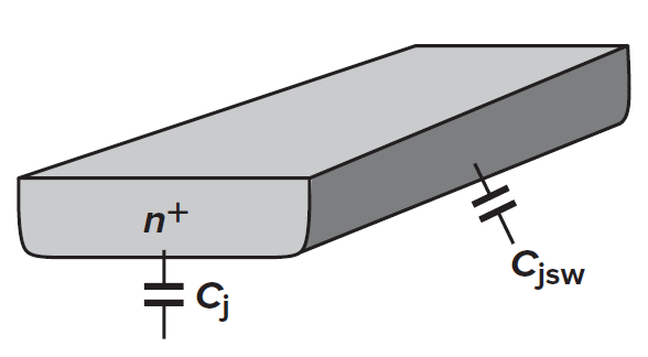
We specify
where
where
In different regions cap. of MOSFET will change. If the device is off, there is no connection between substrate, source and drain. Then
The symbol
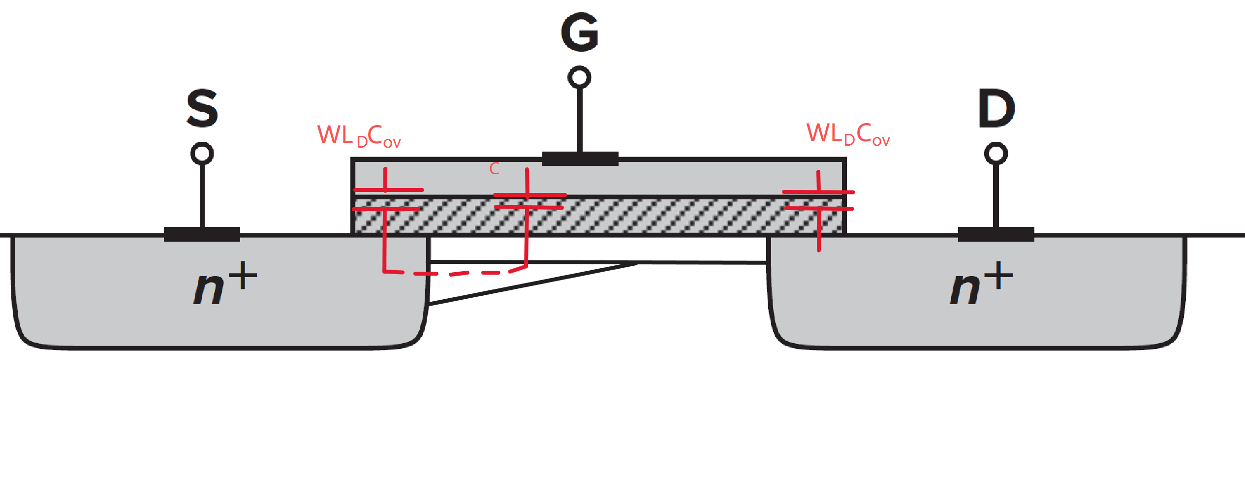
When the device is in deep triode region, i.e.,
In saturation region, the connection between channel and drain is cut off so
and apply current equation in saturation region
Ignore the channel length modulation,
The total charge in the channel is
Plug in
1.6 Small Signal Model
Based on a stable DC point, we can analyze AC signals. The fundamental principle of AC analysis is that we apply a very small signal on a DC signal. Though the DC curve may not be linear, the small range near the DC working point is approximately linear, hence we can apply conclusions in linear systems for AC signals. By the way, we focus on AC signals in most time.
When the device is on, terminal D and terminal S are defined as output terminals. Then
Usually
Recall bulk potential can influence the threshold voltage and current is also related to threshold. It is equivalent to add a current source related to
where
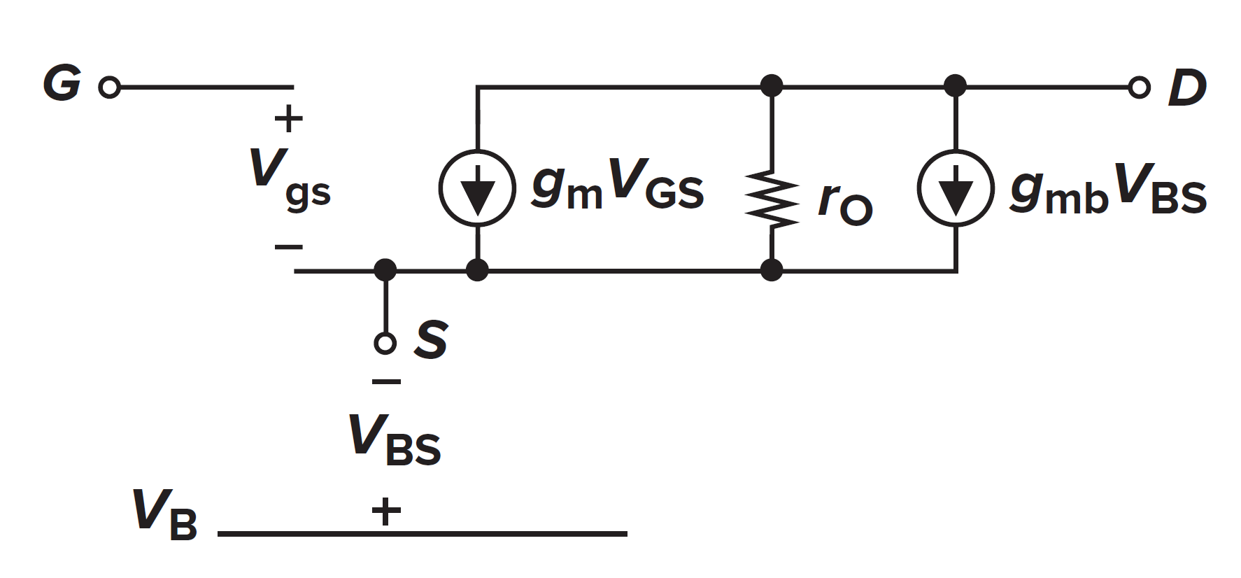
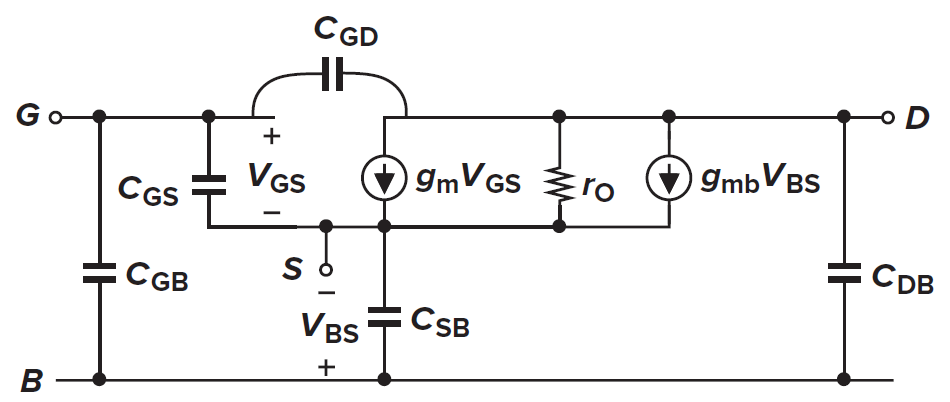
If all cap.’s are taken into consideration, the complete AC model should be
For PMOS devices, since the power supply terminals are equivalent to ground in AC analysis (AC grounding), their AC model remains unchanged. Typically, we mirror-flip them to correspond to the layout where PMOS devices are placed on top in DC circuits.
To recap, we summarize the three important parameters:
: designed by engineers, first order : introduced by channel-length modulation, second order : introduced by body-effect, second order
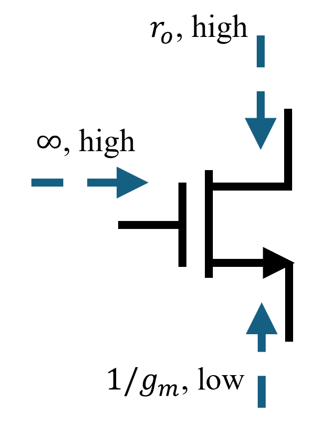
In some cases, we use a simpler conclusion to calculate impedance. For a MOS device, we can summarize the impedance in the view of different ports. This summary can be derived from the small signal model:
2. Single Stage Amplifiers
Note: In the following chapters, we denote “sat.” for “saturation region”, “tri.” for “troide region” and “CLM” for “channel-length modulation”.
2.1 General Considerations
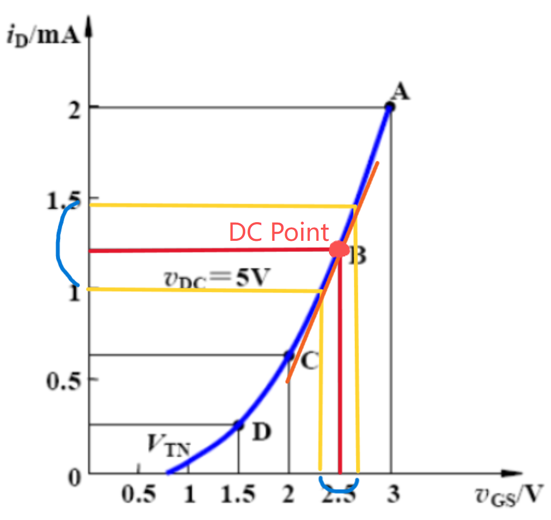
Denote the input signal as
This linear coefficient is called the gain. However, in reality we cannot manufacture ideal things, which means all amplifiers have non-linearity. According to Taylor series theory, we approximate the characteristic by polynomial:
In this general relationship,
We estimate the performance of an amplifier with the following indices: gain, speed, I/O range, power dissipation, supply voltage, linearity, noise and so on. Most of them trade each other so the design is usually a multi-dimension optimization problem.
Our target is to amplify small signals. However, MOS devices have a threshold voltage and may work in different regions. Thus setting a proper DC working point is necessary to confirm the devices work in a desired region.
Before diving into specific amplification circuits, we introduce a general used formula to calculate gain. If a system has a total transconductance
You may find an extra negative symbol in some textbooks, that’s because we apply a different definition. They force the transconductance to be positive for convenience so they have to add an extra “-“ to indicate that the system produces a “inverted phase”. In our definition, the symbol is absorbed by
The formula is easy to prove. According to definition
Since MOSFET can also be considered as an amplification device, we define
as its intrinsic gain to represent its amplification ability.
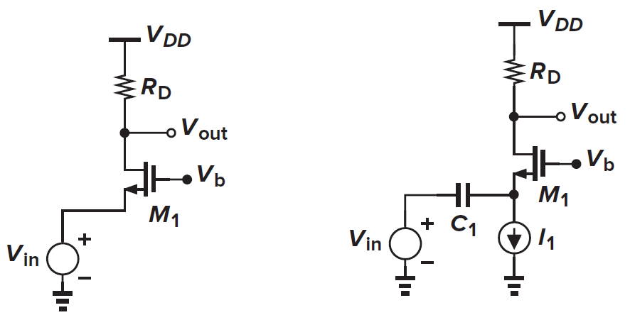
2.2 Common-Source Stage (CS)
2.2.1 CS with Resistive Load
A MOSFET transits its input voltage signal at gate to a current signal. With a load resistance, the current will be transit back to a voltage signal. This fundamental idea introduces common-source (CS) amplifier.
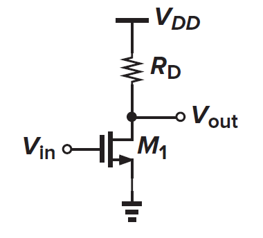
We expect the device to work in sat. and neglect CLM. DC working point is set by the DC component in
The two equations hold in sat. Note that
- Cut-off:
- Tri.:
In cut-off region where
Since the transconductance drops in the triode region, we usually ensure that
We have three methods to calculate voltage gain:
- Partial Derivative on DC Formula
Remember
- Analyze Small Signal Model
- Use the General Formula Directly
Now take CLM into consideration, meaning
Since
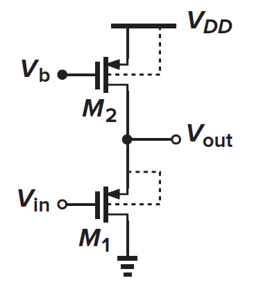
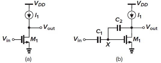
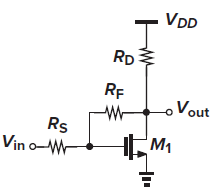
2.2.2 CS Stage with Diode-Connected Load
The basic CS topology has some problems:
The most severe problem is nonlinearity, which is mostly caused by the variation of
Since
But the current source is impossible to be ideal. In fact if it is ideal, DC point is not well-defined. You can try to calculate
If the device is connected like that,
You can figure out the small signal model
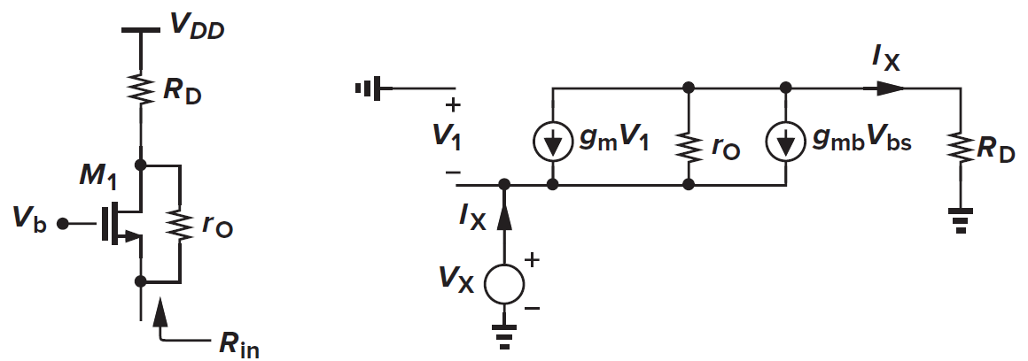
If NMOS serves as a load, we must take body effect into consideration.
From the source, list the current equation
Solve the equation and calculate the impedance
We now study the CS amplifier with an NMOS load. Neglect CLM first
From the output terminal, M2 gives an impedance of
where
The linear behavior of the circuit can also be confirmed by large-signal analysis.
and hence
Take derivative to
Apply the chain rule
Then
It is instructive to study the overall large-signal characteristic of the circuit as well. But let us first consider the circuit with a cap. load. What is the final value of Vout if
The following figure plots the
If the load is implemented with a PMOS, then body effect disappears and the gain is more linear.
With disappearance of
if CLM is neglected. If CLM is taken into consideration, the gain becomes dependent to
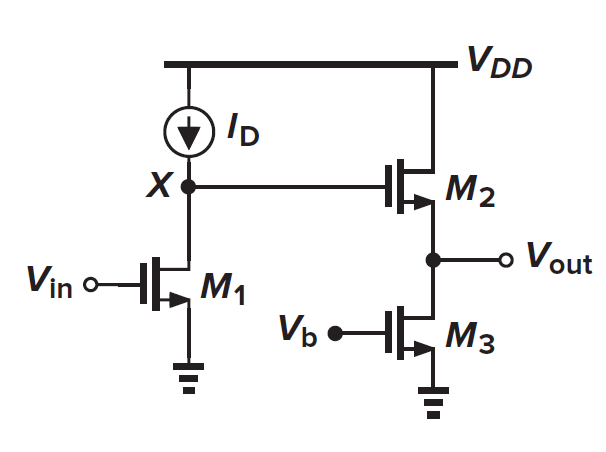
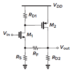
2.2.3 CS Stage with Current Source Load
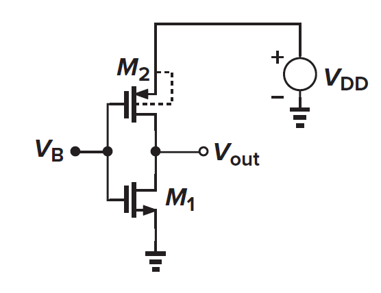
Another mothod to stablize DC working point is to add an extra bias to replace diode-connected MOS.
Obviously the total impedance is
if M2 is biased in sat. However, the
The KCL equation
If the MOSFET up is biased in tri., then it is almost the same as the initial non-optimized circuit. One advantage of biasing in tri. is that you can adjust the resistance value by adjusting
2.2.4 CS Stage with Active Load
If one of the MOS just provides bias, it seems that the gain of that MOS is wasted. Can we make full use of both the two tubes? Yes. The topology is called compensated CS, also known as CMOS inverter.
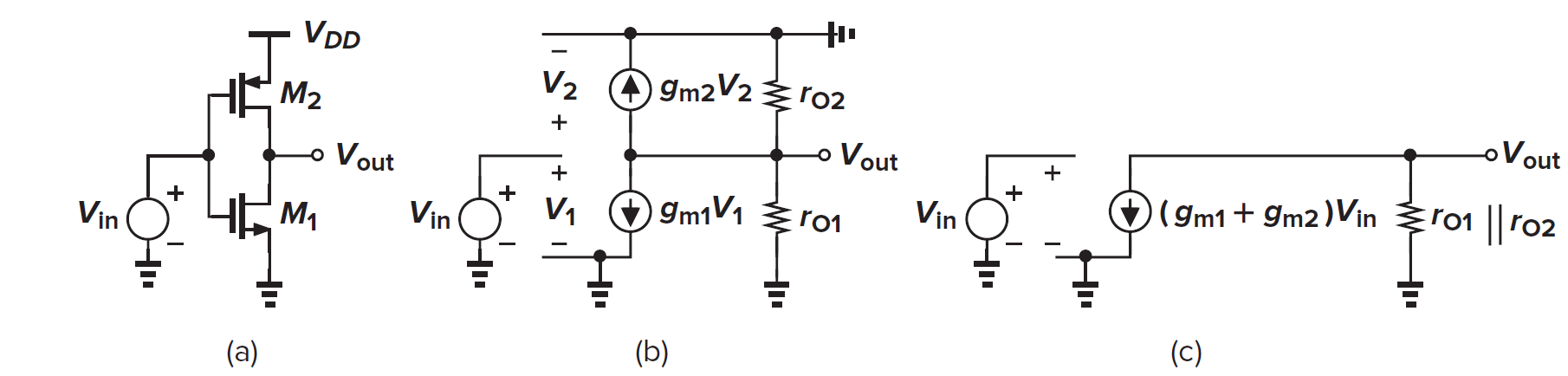
From the small signal model in figure (b), input transconductance
CMOS inverter must solve two critical issues when serves as an amplifier: First, the bias current of the two transistors is a strong function of PVT (Process drift, voltage drift, temperature drift, the three parameters impact the performance and cannot be controlled). In particular, since
And the input range is very small. CMOS inverter sacrifices the power noise and input range to get larger gain. So, this topology is widely used in digital circuits and seldom used in analog circuits.
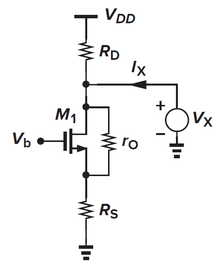
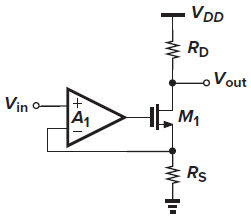
2.2.5 Source Degenerate
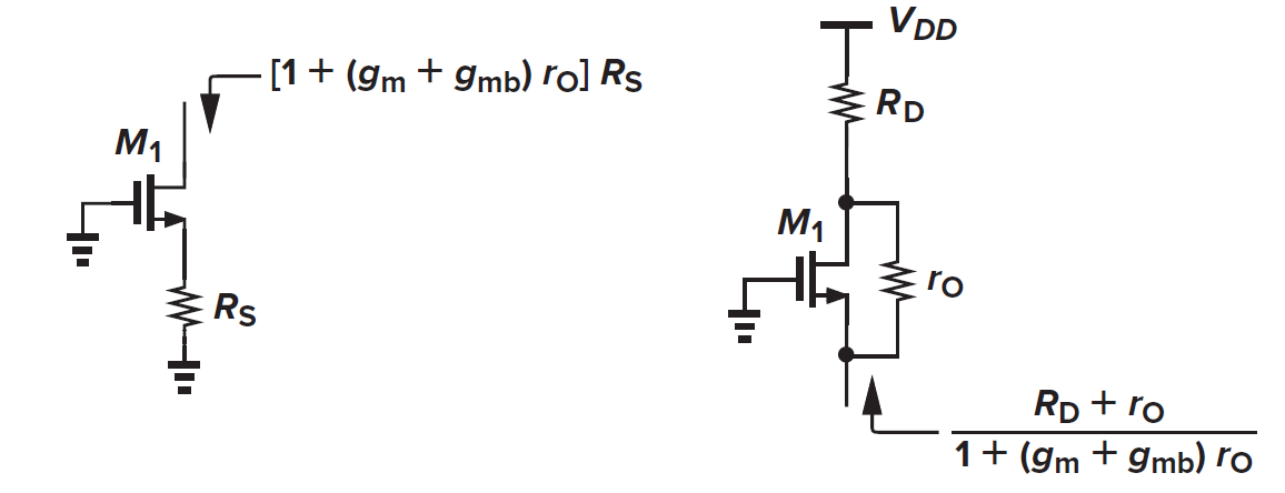
In some applications, the nonlinear dependence of the drain current upon the overdrive voltage introduces excessive nonlinearity. By placing a “degeneration” resistor in series with the source terminal so we can make the input device more linear.
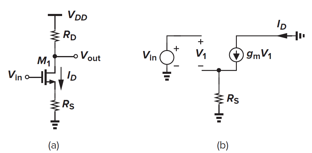
Neglect CLM and body effect. Here, as
Another view of this is the transconductance.
Then
The source degenerate resistor adds an extra
The AC gain is
If CLM and body effect are not neglected, the small signal model is shown below
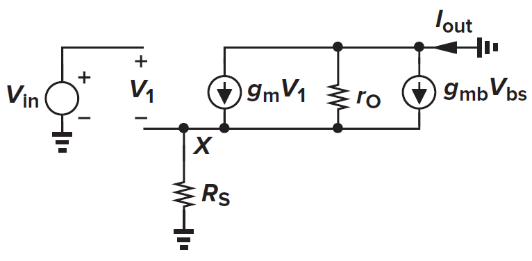
It can be proven that
2.3 Common-Drain Stage (Source Follower, SF)
Our analysis of the common-source stage indicates that, to achieve a high voltage gain with limited supply voltage, the load impedance must be as large as possible. If such a stage is to drive a low-impedance load, then a “buffer” must be placed after the amplifier so as to drive the load with negligible reduction in gain. The source follower (also called the “common-drain” stage) can operate as a voltage buffer.
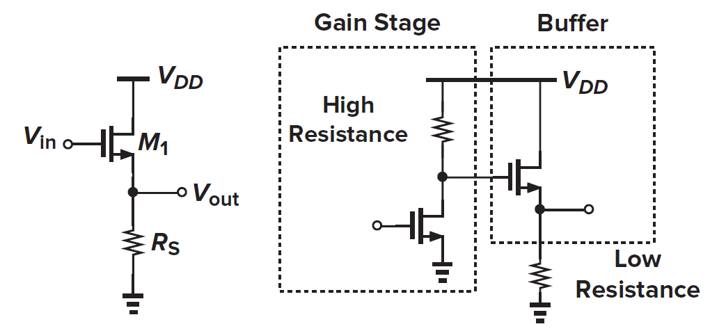
We know CS has a high output impedance mainly restricted by the load resistor. If the input impedance of the next stage is small, the output voltage may drop and only part of the signal can enter the next stage. By applying a source follower, the total output impedance will decrease, therefore has a better driving ability.
we note that for
when CLM is neglected. By taking derivative to
we get
Plug in the transconductance
By using small signal model, the conclusion is easier
As
With the similar reason of CS, we can replace
Usually the current source is implemented with a biased MOS. Equate the two current equations
We can see the input and output is broadenly linear
We apply a feedback loop to adjust
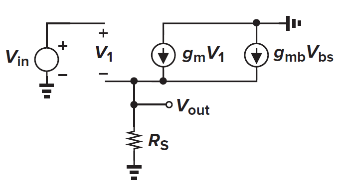
Obviously the SF has a high impedance. We check the output impedance for SF with a load of current source.
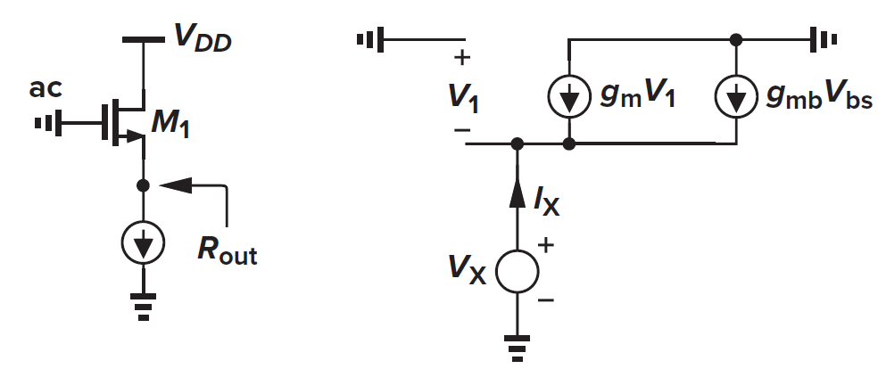
At source point
giving
Since
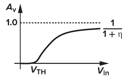
We know the body effect causes part of the nonlinearity. This can be solved if the bulk is tied to source, which means replacing all MOS’s with PMOS.
We must replace all devices because all NMOS’s share the same substrate potential GND. This topology has less nonlinearity but lower mobility of PMOS also yields higher output impedance.
Source followers also shift the DC level of the signal by
2.4 Common-Gate Stage (CG)
It is also possible to apply the signal to the source terminal.
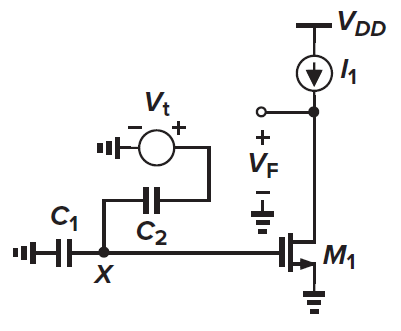
Note that you should give a DC bias in
We also research the DC characteristic first. Take the direct coupled topology. When
and
Clearly as
And as
Interestingly, body effect increases the equivalent transconductance of the stage. From the equation, we can increase
In the capacitive coupled topology, the minimum allowable level of
For the input impedance, we note that with CLM neglected, the impedance seen at the source of M1 equals to
If we draw the small signal figure the result will be the same. Now suppose the current source has a finite resistance (or the DC point will be not-well-defined). The small signal model should be
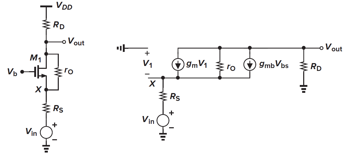
Just apply KCL you can obtain
The gain of the common-gate stage is slightly higher due to body effect.
We now calculate the input and output impedance separately.
At node X
Indicating
Usually
Then set the input voltage to 0 but reserve the source impedance to calculate output impedance.
Draw the small signal model and write out KCL at source terminal
Indicating
This is a very high value. Hence, CG has a low input impedance and a high output impedance. This impedance characteristic is suitable to work as a current buffer or impedance transferer. we loosely say that a transistor transforms its source resistance up and its drain resistance down (when seen at the appropriate terminal).
2.5 Cascode
2.5.1 Classical Cascode
As mentioned in the last section, CG is suitable for receiving a current input. We also know that the CS topology transfer a voltage input to a current input. The cascade of CG and CS is called a cascode topology.
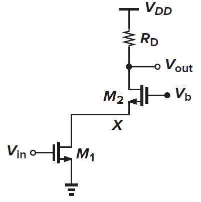
Instead of using the small signal model (of course you can), we view the devices as specific behaviors. With CLM and body effect neglected, we inspect small vairation on
When
By now, we’ve figured out the AC gain without applying small signal model. And such analysis is much more practical in complex systems. As you can imagine, it’s annoying and impossible to draw small signal models in a large scale analog chip with hundreds of MOSFETs.
Now inspect the perturbation on M2, while the input signal on M1 is tied to a constant DC level. In this case M1 works as a constant DC current source. No matter how
Note that
To bias both devices in sat., we must gurantee
For M2 to be sat.,
One of the drawback of cascode is that the output swing is limited.
We now analyze the large-signal behavior of the cascode stage as
As
We still draw the small signal model and try to find the total transconductance and output impedance.
All current flows through
Suppose the AC voltage on the M2 source is
Then
This is a very large value. Thus, cascode is suitable for receiving a voltage input and giving a current output.
Note that the output impedance of M1 from drainis
Finally we get the AC gain
Cascode make full use of the intrinsic gain of both devices. If the two devices are identical,
If body effect is not neglectable,
In fact we can pile CG for many stages to boost the output impedance in a factor of
Rising the lowest
There is a trade-off problems. Recall that
The signal path is that
A cascode structure need not operate as an amplifier. Another popular application of this topology is in building constant current sources. The high output impedance yields a current source closer to the ideal, but at the cost of voltage headroom.
2.5.2 Folded Cascode
Classical cascode has a problem: There are too many devices on one path from VDD to GND, which will limit the swing because we have to gurantee sat. for all devices, increasing design difficulty. To solve this problem, we apply folded cascode.
In folded cascode CS device and CG device are separated to two paths and can be designed separately and independently, but at the cost of double current and quadruple power consumption (bacause both path need a
Usually the folded cascode is biased with a current source
And for
Parallel connection decreases the output impedance and further decreases the gain. This is also one of the cost of folded cascode.
The DC characteristic is
3. Differential Amplifiers
3.1 Single-Ended and Differential Operation
All circuits in the last chapter deals with single-ended signals, which uses the GND as a reference. A differential signal is defined as one that is measured between two nodes that have equal and opposite signal excursions around a fixed potential. This potential is called common-mode signal.
Usually, we can decompose the two inputs:
That is how we decompose common-mode component and differential mode component.
So why we use differential signals, which seems more complicated than single-ended signals? Consider the case below:
Clock line will produce environmental noise on lines in the neighbor through the parasitic cap. between lines. If a single-ended signal is loaded on a wire close to the clock, the signal will be sensitive to the clock perturbation. But if the signal is reassigned on two symmtrically distributed lines, as a differential signal, the perturbation from the clock acts the same on both lines (amplitude and phase). Then, the same noise will cancel each other in the subtraction process to obtain differential mode signal. The noise will be all loaded on common-mode components, which we do not care at all.
3.2 Differential Pairs
3.2.1 Pesudo-Differential Pair
How do we amplify a differential signal? The most simple idea is to amplify the two branches separately, with the same gain
To implement differential characteristics, all components on both devices must be identical. Here, two differential inputs,
Since this is just two CS stages with inverted differential input, neglecting CLM and body effect, the AC gain will be
Because the two paths are almost completely independent, we call this topology pesudo-differential pair.
All problems in fundamental CS stage also appear on this topology. Different CM bias will influence
On the other hand, the pesudo-diffential pair will also amplify the useless CM signals, which impacts the output swing.
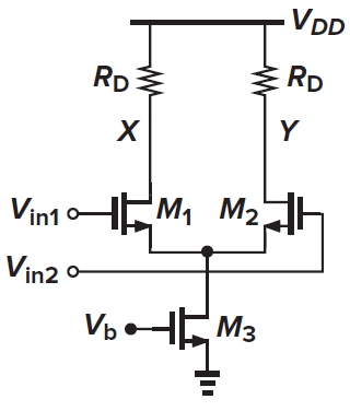
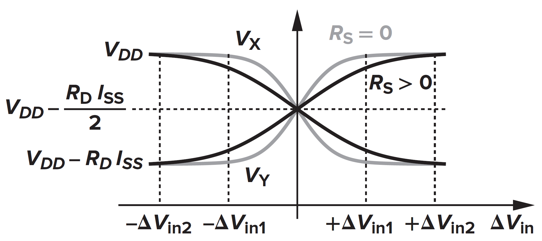
3.2.2 Basic differential pair
A simple modification can resolve the above issue. In this topology the two paths are coupled with a constant current source, usually implemented by a MOS device. This topology is called source-coupled pair.
The source introduces a constraint between the two paths:
We scan
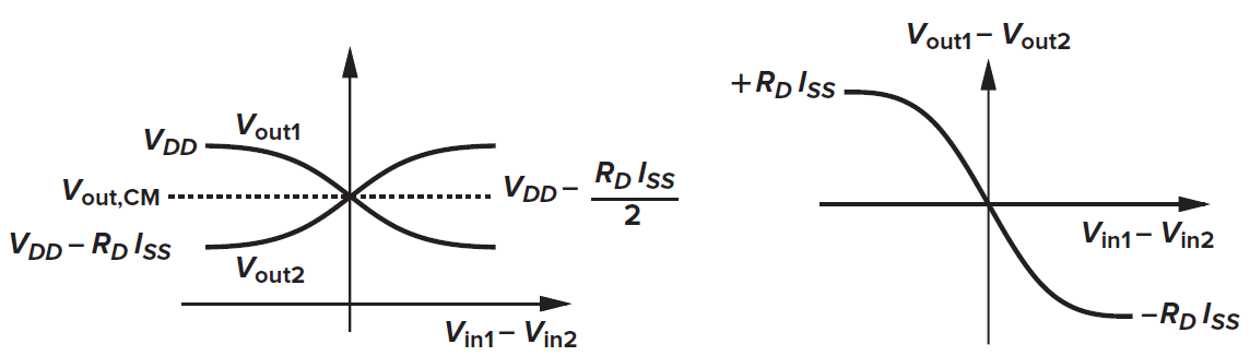
Note that the circuit contains three differential quantities:
Then turn the view to CM behavior. We set
When
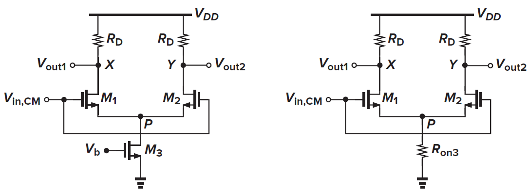
When
Summarize them
With
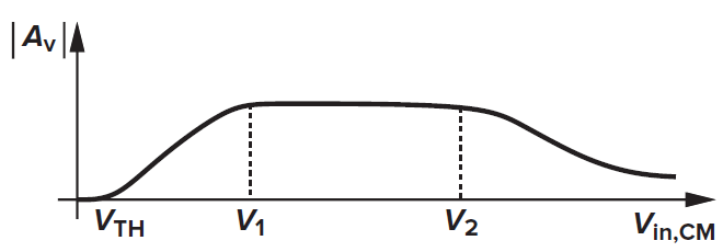
In this region
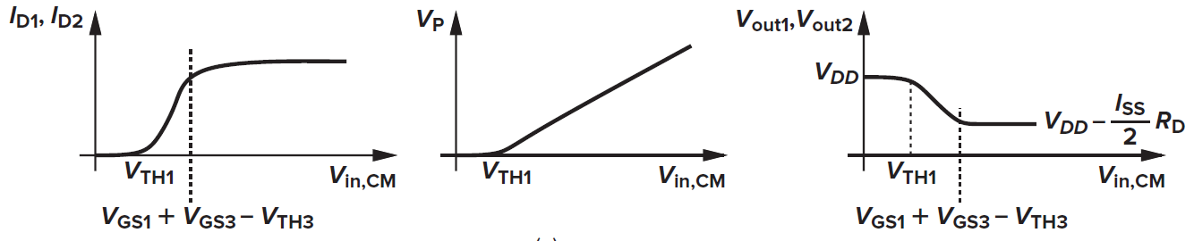
Beyond the upper bound, the CM characteristics of do not change, but the differential gain drops.
Then it comes the output swing. If M1 and M2 are desired to be in sat.
Giving
The upper limit, of course,
Notice that smaller
Now we analyze DM behavior quantitatively. We simply calculate
For a square-law device, we have
and, therefore,
It follows from the preceding definitions that
We wish to calculate the differential output current,
That is,
Squaring the two sides again and noting that
Thus,
Now we obtain the relationship between the differential current and differential input voltage. We can say that M1, M2, and the tail operate as a voltage-dependent current source producing
Before examining further, it is instructive to calculate the slope of the characteristic, i.e., the equivalent
For
Since each transistor carries a bias current of
Let us now examine the expression more closely. If
which yields the same equilibrium
But what happens for larger values of
This value means if you want to make
The value of
Thus,
In equilibrium
Then comes the small signal analysis. We suppose M3 is a constant current source and cut it off in AC diagram. Denote the source terminal shared by the two devices as S and the influence on
Note that the two paths are completely symmetric and inputs are inverted. So
This is an amazing lemma in differential pair. The voltage of node S follows in the CM input but remains constant in AC analysis. We call S a “virtual ground” because it in fact serves as a AC ground. That is because the inverted input is converted to inverted
With the two paths completely symmetric,
then
But PVT may perturb the value of
At node S, the AC current is
leads to (the summed term vanishes because the inverted phase)
giving
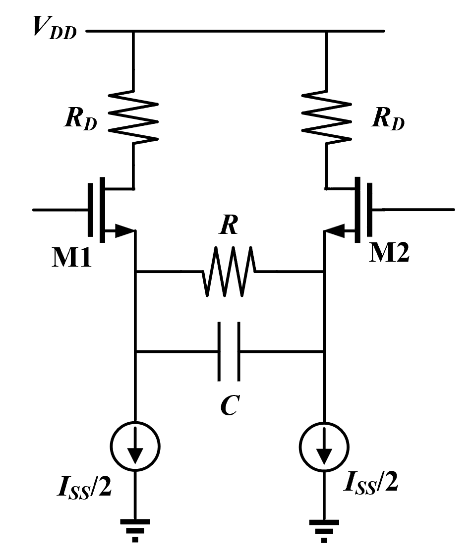
3.2.3 Degenerated Differential Pair
Like the single stage CS, differential pairs can also incorporate resistive degeneration to improve its linearity.
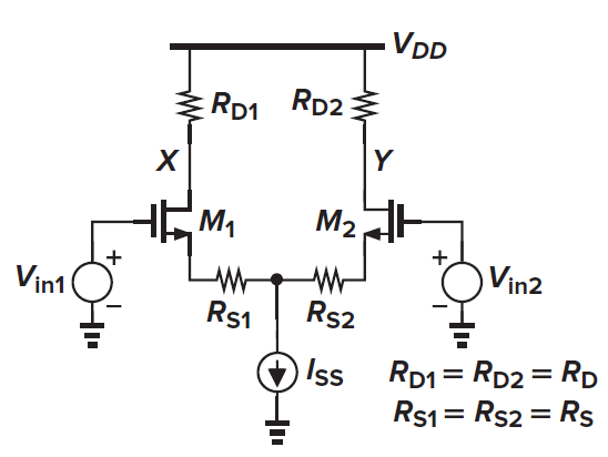
The principle is the same as that in CS stage. To analyze, we introduce the half-circuit technique. This technique is efficient because the two paths in a differential pair are completely symmetric. We analyze common-mode and differential-mode separately.
First comes the common-mode. Suppose M1 and M2 are both in sat., when DM voltage equals to 0, both path has current of
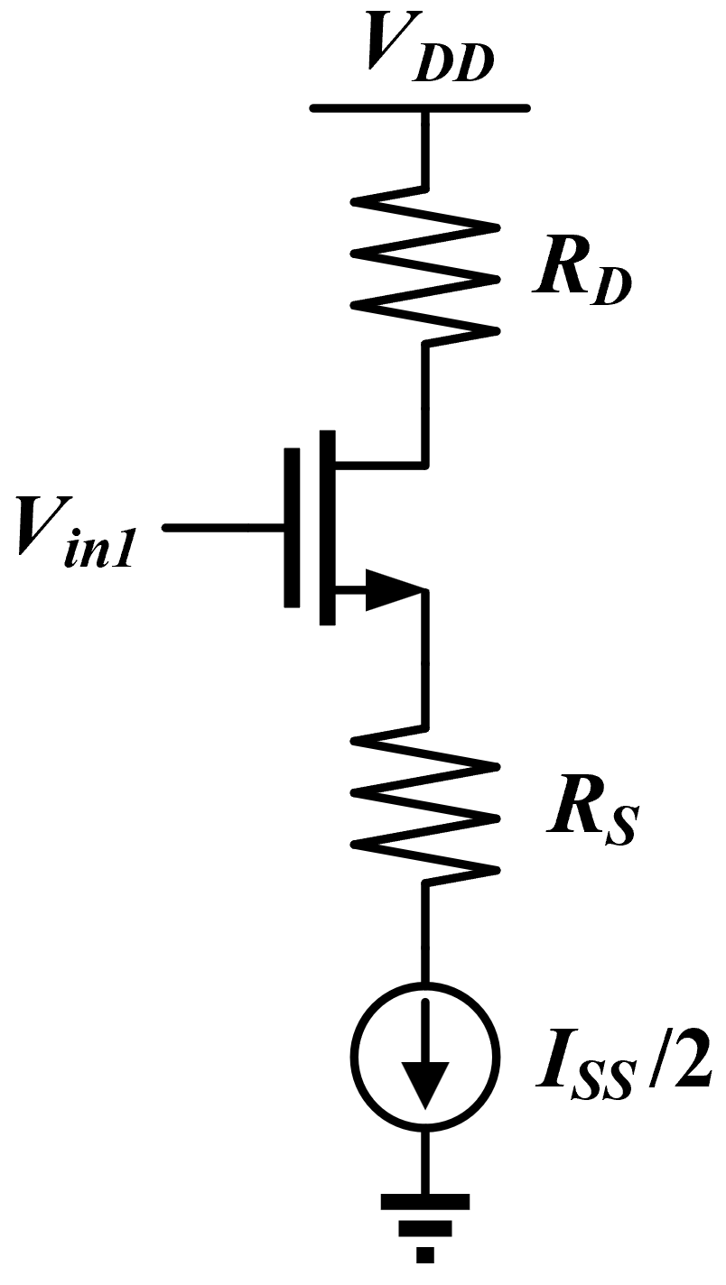
Note that the degeneration reduces the headroom by
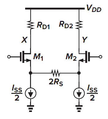
In DM analysis you can see that the resistor
Then the differential mode. Similarly to the analysis in the last section, the node between source resistors is the virtual GND. Then in DM analysis current source vanishes and the DM half circuit is a typical source degenerated CS stage.
Then the small signal gain should be
Thus, the circuit trades gain for linearity. Linearity improvement is shown below.
The degeneration widens the input voltage swing. Suppose the CM input is biased on a proper level. Then increase the DM input until one device is off. In this case another path obtains all current
yields
Note that the first term on right hand side is the input swing before degeneration. So the conclusion is that the degeneration increases the input swing by
We need to clarify the half circuit technique. The essence of this technique is symmetry. Thus, if there are connections between the two symmetric paths, the connection should be divided into two parts. Take the circuit below for example.
For common mode, the voltage between
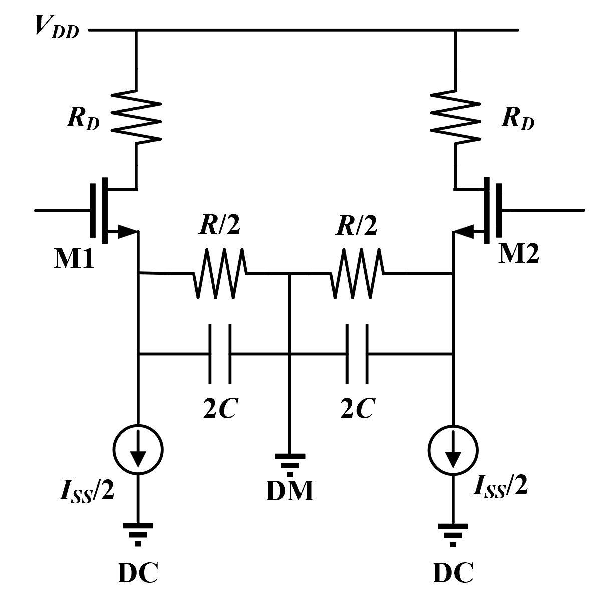
Obviously the half circuit should be
Note that the virtual ground (DM ground) is not the small signal ground (AC ground). The former is based on the symmetry in differential pairs, whose equivalence is still DC ground because DM signal is still large signal. But the latter is based on linearity. Hence, the DM ground should be regarded as DC ground in analysis.
3.3 Common-Mode Response
In reality the circuit will not be ideal. Generally in a differential pair, either the asymmetry or the finite impedance of tail current source will introduce common-mode components in the output differential-mode signal.
First consider the impedance of tail current source.
We first assume that the circuit is symmetric. In each path
By applying half circuit technique,
And by KCL
Combine the two equations,
Then the vairation of
In a symmetric circuit, input CM variations disturb the bias points, altering the small-signal gain and possibly limiting the output voltage swings.
Then comes to the asymmetry. Suppose the
With the conclusion above, the voltage on the two output nodes are
Thus, a common-mode change at the input introduces a differential component at the output. On the other hand, the MOS devices are usually not symmetric. Owing to dimension and threshold voltage mismatches, the two transistors carry slightly different currents and exhibit unequal transconductances. Writing
and
We then obtain the output voltages as
The differential is
In other words, the circuit converts input CM variations to a differential error by a factor equal to
Generally, to measure the rejection performance of a differential circuit, we define a parameter called common-mode rejection ratio (CMRR).
If only
3.4 Differential Pair with MOS Loads
The load of a differential pair need not be implemented by linear resistors. As with the common-source stages, differential pairs can employ diode-connected or current-source loads.
The half circuit indicates that it is a CS stage with MOS load. Recall the last chapter, with small signal model
Giving
Replace
The diode-connected loads comsume voltage headroom thus creating a trade-off between the gain and the output swing because the rising of
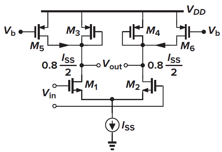
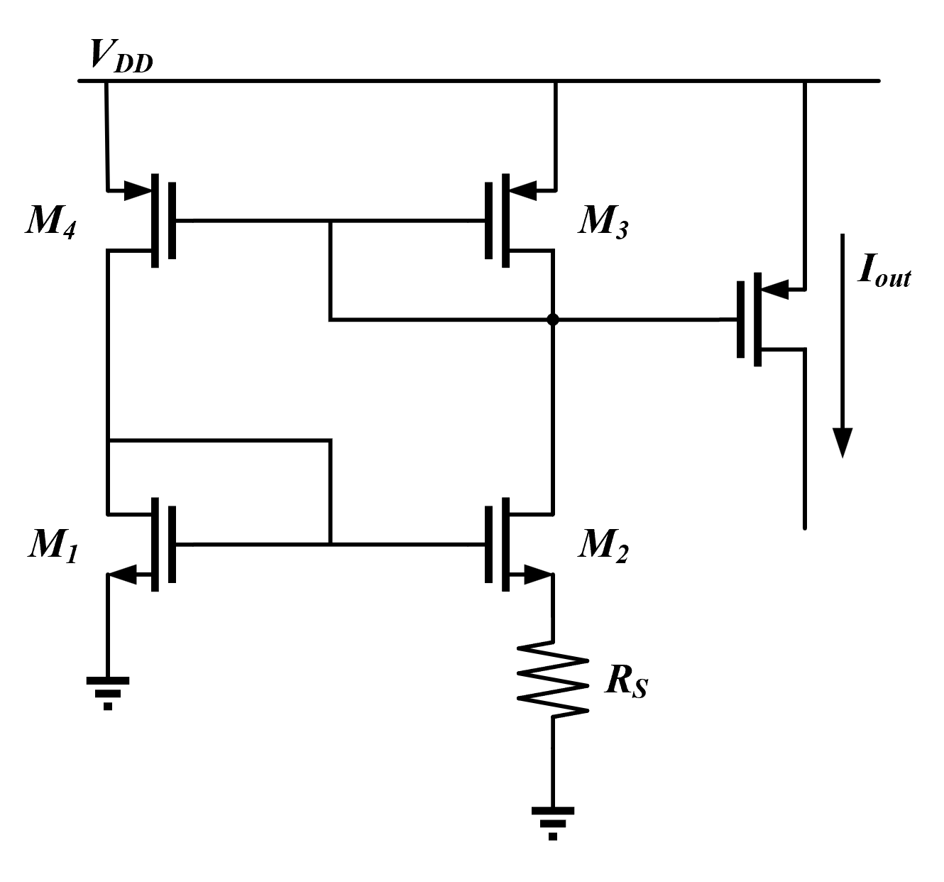
In this structure M5 divided 80% of the
3.5 Gilbert Cell
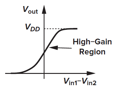
The small signal gain of a differential pair is a function of
Note that if we converse the definition of the output terminals, the gain becomes positive
Then, to obtain the gain varying continuously from negative to positive, two pairs should be used.
If we add the two output signals together
If the two pairs are completely identical,
Varying
But how to add the differential pairs together? Note that
then we connect the related terminals together (because the
Now, the bias contains two independent variables,
4. Biasing Techniques
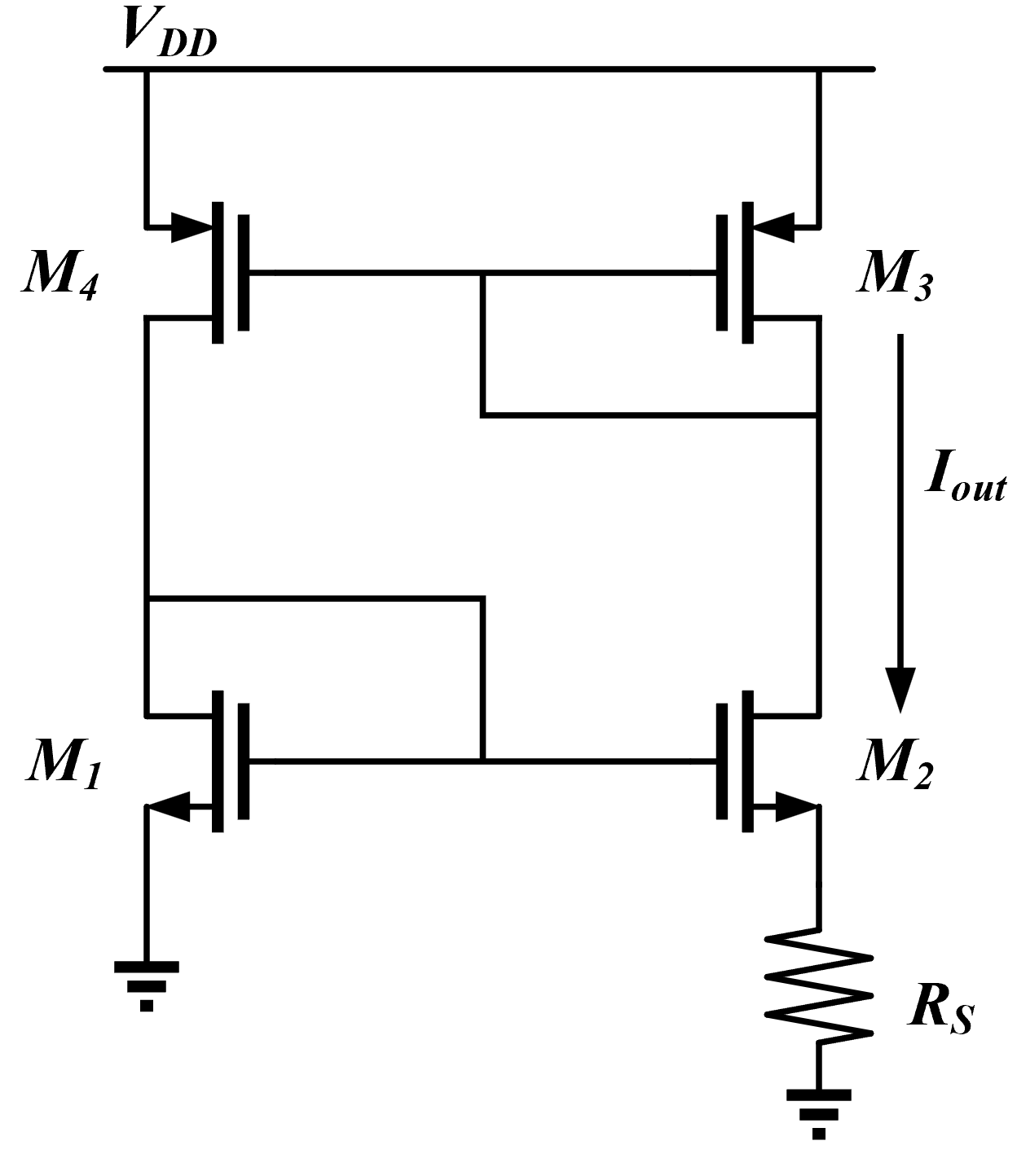
4.1 Current Mirrors
In the chapters above we use biasing voltages or currents many times. For example, the tail current in a differential pair. To generate a current, we have two ideas: +
- Generate a biasing voltage on the gate of a MOS device, which works as a current source
- Copy a reference current
The first idea is not usable. To know why, take the following circuit for example:
In this circuit
It seems simple, but completely not applicable. First the current varies with
Another point is that generating voltage level by resistor divider is also a terrible option because the voltage changes with your load.
Then we should apply the second idea: copying a reference current. This function is implemented by current mirror. The basic idea is that for a MOS device
Then we have the following topology: current mirror.
M1 is diode-connected so it is guranteed to be in sat., then
obtaining
If the two devices are identical,
Generally current mirrors employ the same length for all devices to minimize errors due to side diffusion. And widening the channel will introduce extra error in processing (identical devices contains less error in processing). Hence, in practice people stack identical devices in parallel to equate the effect of directly widening the channel.
When it comes to fractions (like
But the CLM will also influence the output current. With CLM neglected, a term
To compensate for changes in
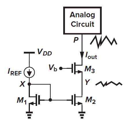
The bias can be provided by
For M1,
But cascode consumes output headroom. To make all devices sat., the minimum allowable voltage at node P is
If
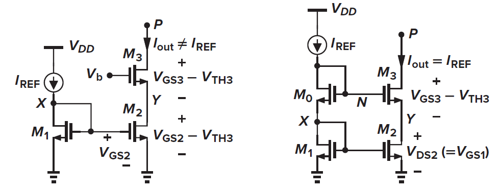
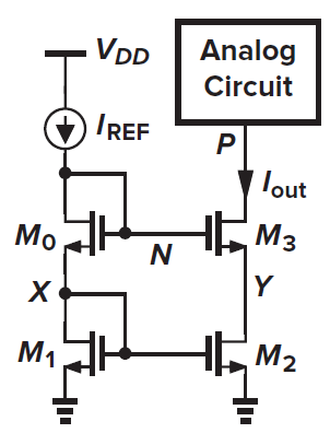
Obviously the cascode wastes one threshold voltage headroom. To solve this problem we need to decrease the voltage at node Y (not necessarily X because M3-M2 is the output path and the headroom is independent of M0-M1 path.). We move the output path away and the original path is reserved to decrease the node voltage.
where
With this size relationship
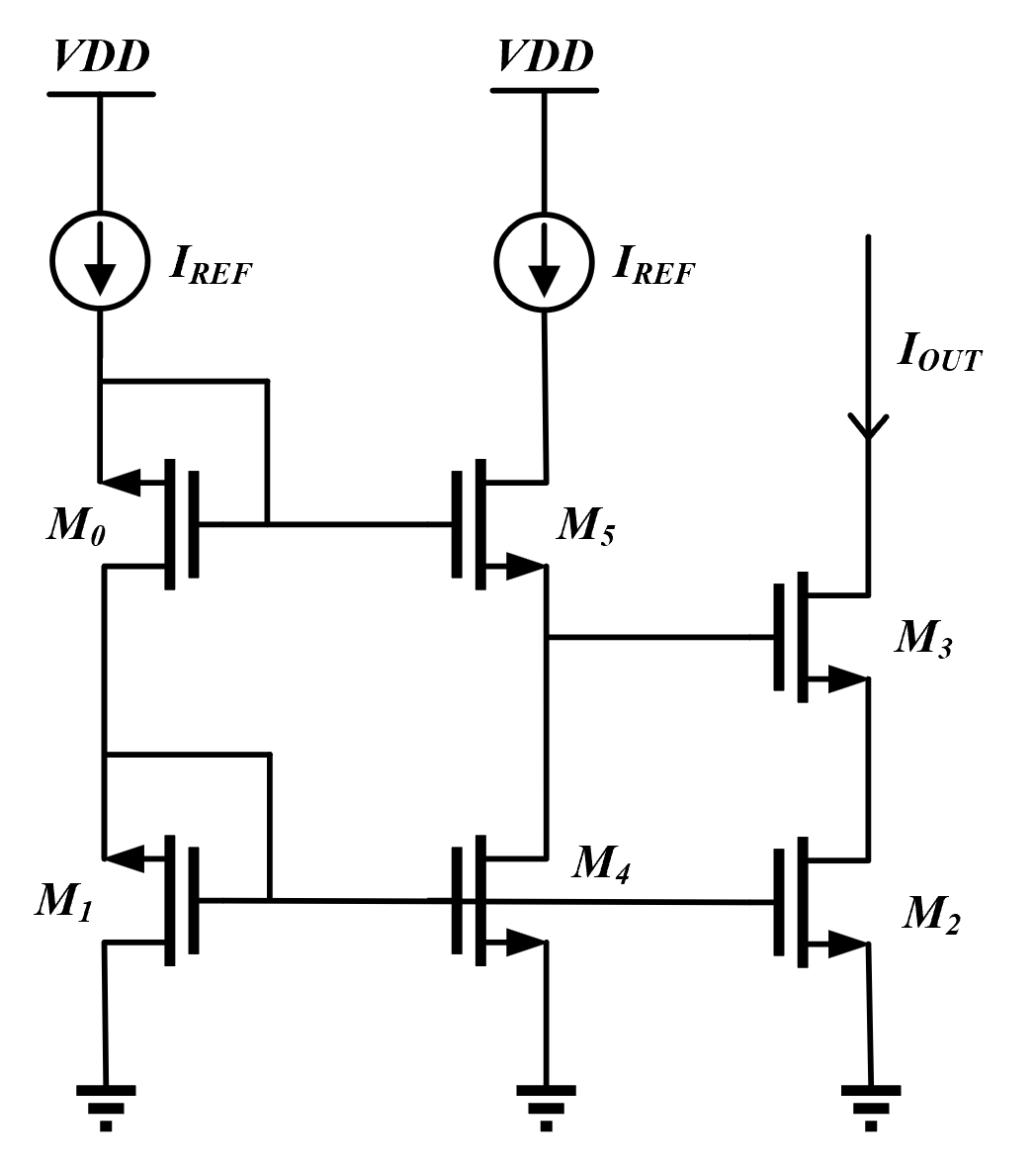
4.2 Current Generation
But where does the reference current come? Then we need the current generation circuit.
The following is called constant transconductance current source.
where
Based on this condition, the current through M4 (serving as
In REF path
while in OUT path
meanwhile
PMOS mirror forces that
or
where
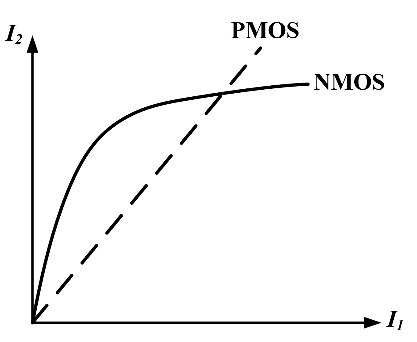
A solution of 0 means the circuit can be completely open. A circuit with two distinct solutions is typically referred to as having a degenerate solution. In fact, the trivial solution is unstable. Upon even a slight disturbance, the current will immediately increase, eventually reaching the non-trivial solution and settling into equilibrium.
In the following figure, suppose the
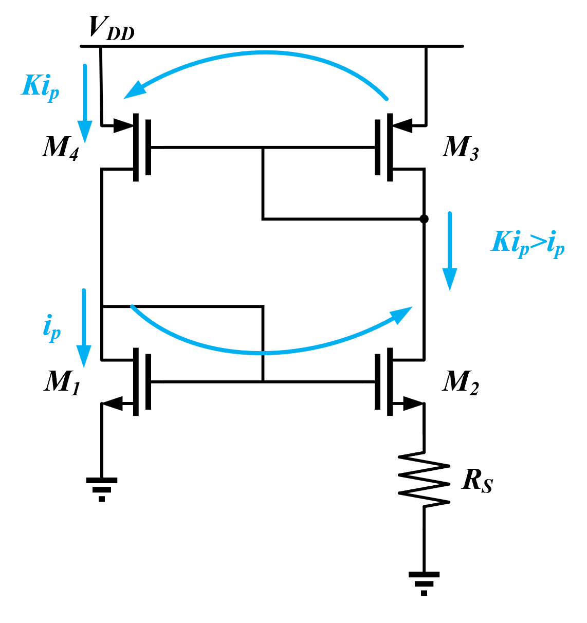
To avoid body effect, the load can be placed between the PMOS and VDD.
To enable the current output, copy it again
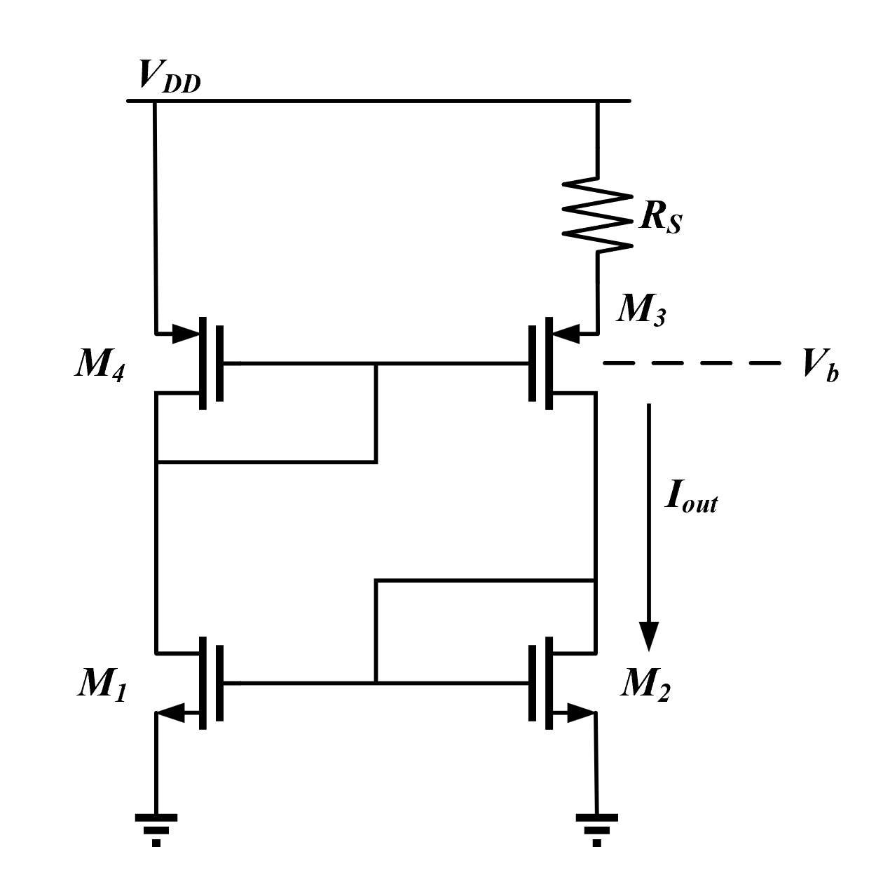
4.3 Operational Transconductance Amplifier (OTA)
Generally we need a single-ended signals. In this case classical differential amplifier will be not applicable. Then we need operational transconducance amplifier (OTA) to transform the differential signals to single ended ones. OTA is implemented by replaceing the classical load with current mirrors.
The idea is to mirror the current in one path to another and substract. Suppose current in M1 and M2 are
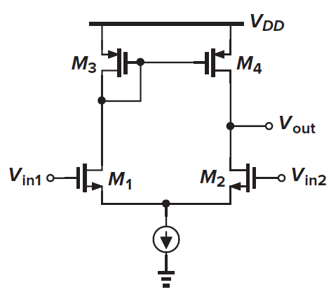
When the current source is implemented by a NMOS, the circuit becomes a typical 5-transistor OTA.
DC analysis of OTA
If
AC analysis of OTA
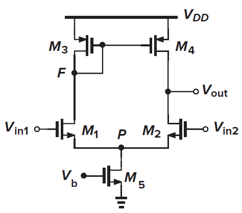
Since the circuit is not completely symmetric, so the node P is no longer a precise virtual ground. We can check the non-symmetry through impedance calculation.
Let’s review the small-signal model of a MOSFET. The impedance from the drain to AC ground is
Then in small signal model of OTA, when VDD becomes AC ground, at node F the impedance relative to ground is
Since
When two large resistors are connected in parallel, their combined resistance remains very high; therefore, the output impedance of this circuit is very high (which is why it is suitable for driving current-driven loads). Because the impedances differ, the voltage swings at the two nodes are also different.
We assume M1 and M2 are identical, thus
By the way we have known
If the effect of the current mirror is taken into consideration, the entire small signal model is
I’m lazy to calculate the complex fucking equations, the result is
Headroom Issue
To make the current mirror (mainly M4) sat. (or deeper to keep precise mirror),
Then to make M4 sat.
Common-mode Properties
Connect two input terminals, then the current through two paths are equal. Since M1 and M2, M3 and M4 are separately identical, the voltage on node F and out must be the same. Thus, the two nodes can be virtually shorted.
The analysis is similar
thus
Then
Mismatch Issue
In case there is mismatch, for example M1 and M2 are not completely identical, the output will be distorted. Suppose the common-mode voltage changes a little
Meanwhile
Then
Compared to the non-mismatch result, this result contains the additional term
the effect of transconductance mismatch on the common-mode gain.
Power Supply Rejection
OTA has terrible PSRR (Power Supply Rejection Ratio), i.e., it can almost not resist the noise on supply. That is because for M3, the noise of supply rail is a source following process. Thus, any variation on
5. Frequency Response
5.1 Poles and Zeros
For a electric system, its transfer function can be expressed as
where
Note that
A zero point term,
Then a zero point on the right half plane (RHP) contributes to a 20dB/dec slope increasing of amplitude. The zero point also contributes a phase shift of
A left half plane (LHP) pole affects the transfer function by
A LHP zero contributes 20dB/dec amplitude slope increase, but
Whether it is a zero or a pole, the phase shift is exactly 45° at the frequency corresponding to that zero or pole; only when the frequency is much higher than that frequency does the phase shift gradually approach 90°. Different zero-pole effects can be superimposed.
5.2 Miller Effect
An important phenomenon that occurs in many analog (and digital) circuits is related to the “Miller effect,” as described by Miller in a theorem. This theorem is usually used to simplify loops.
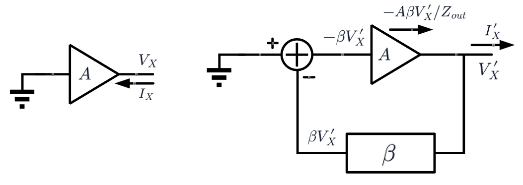
Miller’s Theorem: If an impedance
The proof is trivial:
Generally, the fixed voltage ratio (gain) is provided by the main signal path, for example an amplifier. Thus, Miller equivalence is only suitable for signal path parallel to the main path.
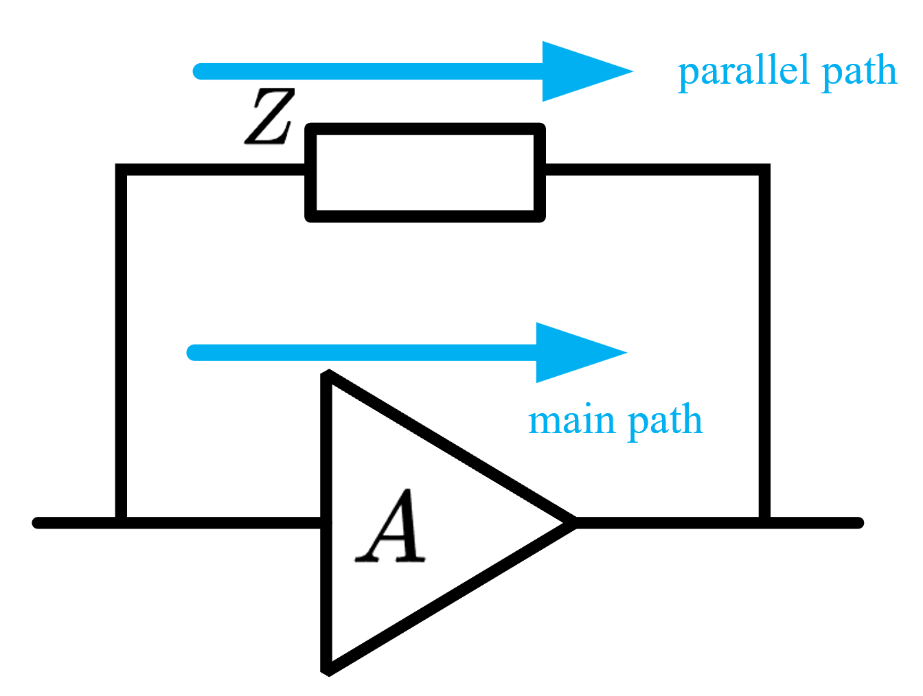
In reality, gain is usually frequency‑dependent. Fortunately, for many approximate analyses, precise circuit characteristics are not required. Therefore, as a simplification, engineers often use the low‑frequency gain to compute the Miller capacitance and then apply this result to high‑frequency cases, even though the Miller equivalence strictly assumes a frequency‑independent gain.
If applied to obtain the input-output transfer function, Miller’s theorem cannot be used simultaneously to calculate the output impedance. To derive the transfer function, we apply a voltage source to the input of the circuit, obtaining a value for
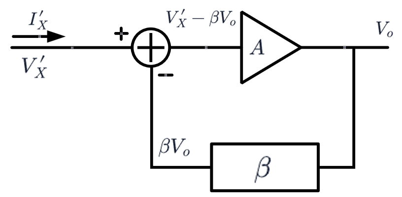
Generally, a cap. on a feedback loop introduces a zero. But applying Miller equivalence may eliminate the zero. Take the example below:
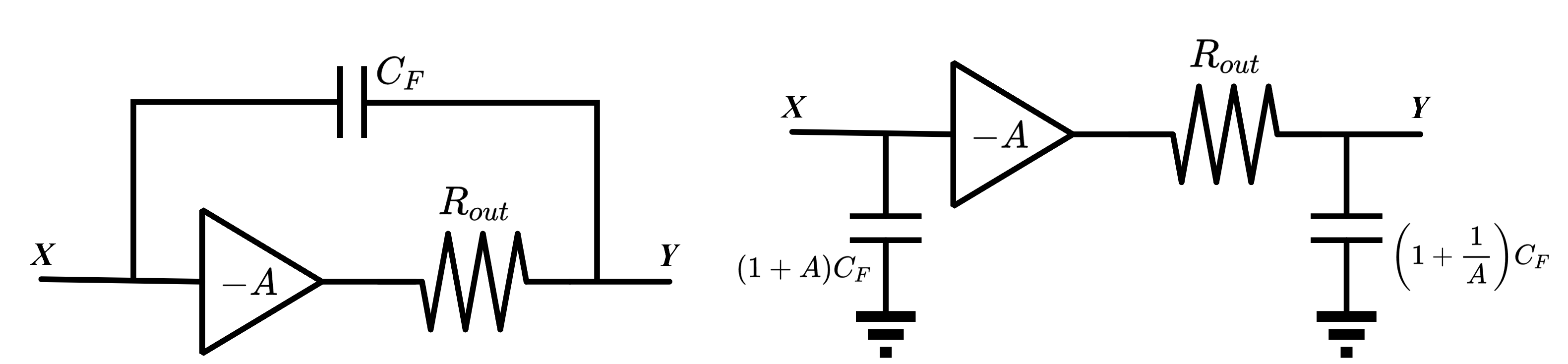
We suppose
There is one pole
But when we apply Miller equivalence, like the right figure, the transfer function becomes
The pole is
We can see that the Miller equivalence may drop a zero point. By the way, the Miller’s result does not completely match the precise result. Thus, we usually apply Miller effect to estimate the pole point, not to calculate the entire transfer function.
Generally, pole points can be estimated by nodes. Take the example above, the right figure. It is obvious that the output node is decoupled with any other parts in the circuit. The node connects only a resistor and a capacitor, forming a low-pass network. Thus, the lowpass network introduces a one-order pole point.
Connecting poles with nodes is a method that is usually used.
To approximate the dropped zero, ground the output terminal and impose the output current to be 0.
5.3 CS Stage
Now we need to take the parasitic cap.’s into consideration.
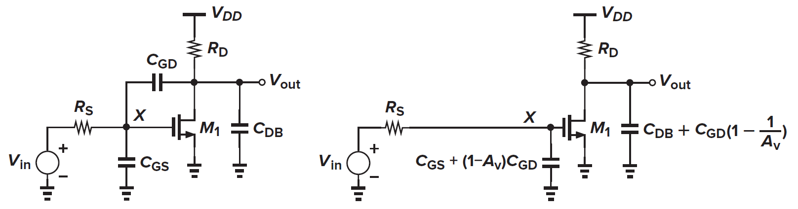
The main path is obviously the MOSFET, so the
and output node
Do not forget to take the dropped zero back.
Since
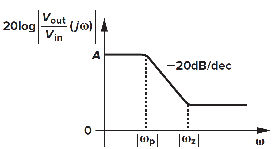
The first pole is called the dominant pole, which affects the frequency response most severely.
If you calculate from the small signal model directly, you will get a transfer function in the following form:
In most circuits the distance between poles are very large, so you do not need to solve the denominator equation precisely. Instead, approximating with Vieta’s theorem:
Approximate
5.4 CG Stage and Source Followers
CG frequency response is simple because there’s no loop if CLM is negligible.
At input node, the source impedance
The output node is simple
If
For source follower, since its gain is approximately 1, not very large, so it exhibits some interesting properties.
The complete transfer function is
If the two poles are assumed far apart, then the lower one has a magnitude of
Note that if you want to apply Miller effect, you will find that the Miller-equivalent cap. vanishes because the gain
Let us now calculate the input impedance.
Then
At low frequencies,
At hight frequencies,
Note that there is a
Neglect the load cap
yielding
At low frequencies
5.5 Cascode
Cascoding proves beneficial in increasing the voltage gain of amplifiers and the output impedance of current sources while providing shielding as well.
At node A,
At node X, its impedance is the M2 source impedance
The node Y is easier. With CLM neglected, impedance
5.6 Differential Pair
The pole estimation follows the same pattern and we do not repeat them. What special in differential pair is CMRR. Consider a complete differential pair with passive load.
With
Then it comes to the common-mode response. The circuit becomes
The cap can be absorbed into one impedance
KCL gives
obtaining
The output differential voltage
i.e.
Notice that the CMRR has one pole of
When it comes to active-loaded differential pair (OTA), the result is much more complex.
The figure on the right is obtained by replacing
But in practice you can still estimate poles with our classical method. At output node
At input node, neglect
6. Noise
6.1 Noise Theory
Noise is a random signal that cannot be predicted even if all signals in the past are known. Thus, the research of noise must be completed with statistical models. In most cases the average power is predictable. We observe the signal in a period of time
But noise is a random signal. So the average power changes with the selection of
To adapt all types of signal (like current), we remove the resistance on the denominator.
This concept becomes more versatile when frequency spectrum is introduced, and also more practical. In the view of frequency domain, the spectrum should give the same energy (power) as that of the time domain.
The
Obviously, the
Theorem: If a signal with spectrum
The absolute value on the transfer function is introduced by the nature that PSD carries energy and energy must be positive, while the square comes from the squared dimension of
For real signal
The common effect of two noise source is not always independent. Let’s add two noise signals and check the power
If the cross term vanishes, the two noise sources are called uncorrelated; otherwise they are correlated.
In most cases, noise sources are uncorrelated or we can say they are independent. For example: the noise introduced by two lumped resistance. Correlated noise always originates the same generation or follows a fixed transfer relation. For example the power supply noise applied to different stages finally compiles to the same output. They comes from the same generation so these noise sources are considered correlated.
Sometimes the amplitude is also important. Then we take the square root of the PSD, obtaining the amplitude spectrum. But note that the amplitude is not
To measure the noise performance of a system, we introduce a index called “signal to noise ratio” (SNR), defined as
SNR is usually measured in decibel (dB)
Keep in mind that the factor is 10, not 20, because SNR is a power ratio. The factor 20 is used for amplitude ratios. The factor 2 comes from applying the logarithm to a squared quantity (since power is proportional to the square of amplitude).
6.2 Thermal Noise
Resistor thermal noise
Lumped resistor introduces noise due to the thermal fluctuation of its atoms. This type of noise is called thermal noise. Since fluctuation is independent of the frequency, the PSD must be flat. Noise with this feature is called white noise. Generally, the resistor thermal noise can be expressed as
where
Since we can express the noise with voltage amplitude (obviously through the Thevenin’s theorem), we can also express the noise via current, though Norton’s theorem.
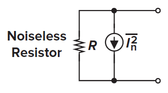
To equate with the Thevenin model, the current noise express must be modified
MOSFET thermal noise
MOSFETs also exhibit thermal noise, mainly introduced by the DS resistance. The channel thermal noise can be modelled by a parallel current source between drain and source.
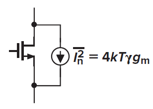
With noise current PSD
The
Another noise originates from the distribution resistance on the gate. For a relatively wide device, the channel noise is typically negeligible and the gate resistance becomes dominant. Now take a example of the simplest MOSFET.
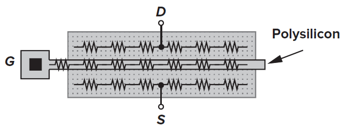
Suppose the total end‑to‑end resistance of the gate polysilicon (from left to right) is
The transconductance contributed by a small section
The resistance from input to
Then the total current transfered from gate voltage noise is
Hence, the distributed resistance on the gate can be equated as a lumped resistance valued
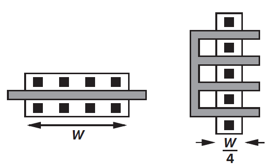
Suppose the total end-to-end resistance in the first layout is
6.3 Flicker Noise
This type of noise appears in the channel of MOSFETs. Since the silicon crystal cannot be completely perfect, it must contains some defects. When the channel turns on, these defects may capture and release electrons randomly. In the external view, the electron number is changing randomly in the device. Noise caused by the defects is called flicker noise.
Obviously, slower electrons are more easily to be captured and released, while faster ones are more difficult. Thus, the PSD of flicker noise is not flat. Instead, the
Superposed on the gate.
It is believed that some other phenomenons also contributes to the flicker noise. So the expression may be more complex in reality. But up to now no one knows why.
Obviously, the MOS is influenced by the thermal noise and flicker noise at the same time. In low frequencies band, flicker noise is dominant while in high frequencies thermal noise plays the most important role. The turning occurs at the frequency of
This frequency is called corner frequency
6.4 General Noise Model
Consider a general circuit with one input port and one output port. How do we quantify the effect of noise here? The natural approach would be to set the input to zero and calculate the total noise at the output due to various sources of noise in the circuit. This is indeed how the noise is measured in the laboratory or in simulations.
But the output-referred noise does not allow a fair comparison of the performance of different circuits because it depends on the gain. Considering only the output noise, we may conclude that as the gain increases, the circuit becomes noisier, an incorrect result because a larger gain also provides a proportionally higher signal level at the output. That is, the output SNR does not depend on the gain.
To remove the puzzle caused by the gain, we equate all the noise to the input terminal instead of the output terminal, obtaining the input-referred noise
The input-referred noise indicates how much the input signal is corrupted by the circuit’s noise. But it cannot be measured by experiments because the input-referred noise is just a mathematical equivalence. Physically the sources are still distributed in the system, not on the input terminal.
But there is still a problem: If we apply a simple Thevenin model (only one voltage source), it implies that the output noise vanishes when the output impedance of the last stage is much larger than the system input impedance, which conflicts with the experimental observations. A simple Norton model also encounters the same problem when the source impedance is much smaller than the input impedance. To solve the problem, we have to apply the two models at the same time: An input-referred noise is composed with a voltage source and a current source.
To illustrate in detail, take the example of the CS stage, and ignore the flicker noise.
The first figure displays the effect of voltage component. The output noise is a superposition of thermal noise of
The gain is
To obtain the input-referred current, we must include the input cap. The output is generated by the voltage raised by the current on the cap.
Hence
The result is
Suppose the source impedance is
From the equation above, we can see that if
We conclude that the input-referred noise current can be neglected if
Some may doubt that the two sources overlap in some of the sources in the system and become correlated. Initially we suppose they are uncorrelated, and through two boundary conditions, we solved the sources. Mathematically, the two sources have unique solution. So it’s not necessary to worry about the source overlap.
6.5 Noise in Single-Stage Amplifiers
Since the gate of MOSFET usually serves as the input terminal, while the gate owns high impedance. Thus, the current source of noise encounters some problems. To solve the “high impedance problem”, the current source should be moved to some other places. This method is only applicable to single-stage amplifiers.
Lemma: The voltage source of noise
Since the circuits have equal output impedances, we simply examine the output short-circuit currents. If the output current is provided only by the current source (fig c),
Solved
If provided by voltage source only,
Solved
Now plug in
CS-Stage
We have calculated it in the example in section 6.4. We do not repeat it again. Now we just focus on the flicker noise.
Since the flicker noise can be superposed on the gate directly, the total input-referred noise is
To reduce the noise, the transconductance should be maximized.
CG-Stage
A CG-Stage serves as a current buffer. On the output terminal, the noise is composed with the thermal noise of
Recall that the gain of CG-stage is
Then open the input terminal. Since the source terminal is open, the MOS noise flows to the source and encounters an infinite impedance, raising the source voltage abruptly and suppresses the
For flicker noise, it is originally applied on the gate of MOS, i.e.,
Divide the gain to obtain input-referred voltage
The input-referred current is more obvious
Source Followers
The noise comes from both devices. Neglect the flicker noise. The output noise
The gain of a source follower is
Then transfer back to the input
Cascode Stage
M2 vanishes because at node X the noise current of M2 is forced to equate that of M1.
6.6 Differential Stages
Differential Mirror
Since the current noise on the two paths are not correlated and no one can say they owns inverse phase, the source node cannot be regarded as a virtual ground. So the half circuit equivalence is not applicable here.
Suppose the
Transfer to the input, the gain is
The single-ended noise should be included into the differential signal
The flicker noise works the same
Then take the noise of
Suppose
Thus, the noise of
Current Mirror
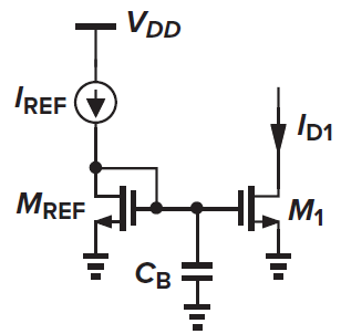
The REF MOS introduces a thermal current noise
Note that the REF MOS is connected in the diode mode. Look from the gate (in fact from the drain), the impedance is
The input of M1 is first processed by this transfer function and then becomes the output current noise through
Hence the noise caused by thermal noise is (include the thermal noise of M1 itself)
As for the flicker noise, just replace the
OTA
M1 generates a thermal noise
Superposed with the two flicker noise
then these voltage noise will be transferred to current noise in M4-M1 path through
Suppose M1 and M2, M3 and M4 are respectively identical, then the current can be simplified
With the flicker noise of M1 and M2
The output impedance of OTA is
Dividing the result by
Don’t forget the flicker noise of M1 and M2
7. Feedback
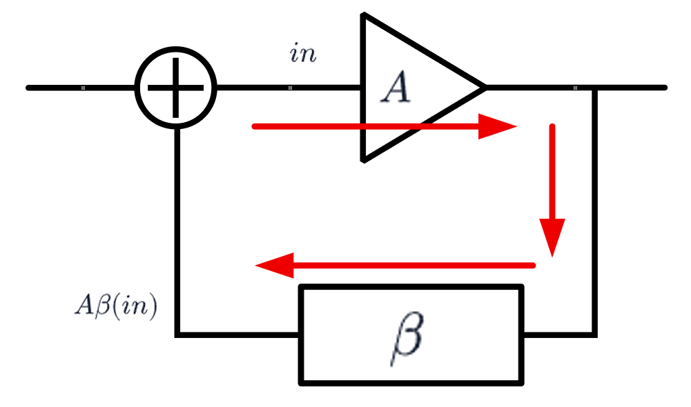
7.1 Primary Theory of Feedback
Negative feedback is widely used in analog circuits. It allows high-precision signal transfer, smaller linearity and better stability. The following figure demonstrates a typical diagram of negative feedback.
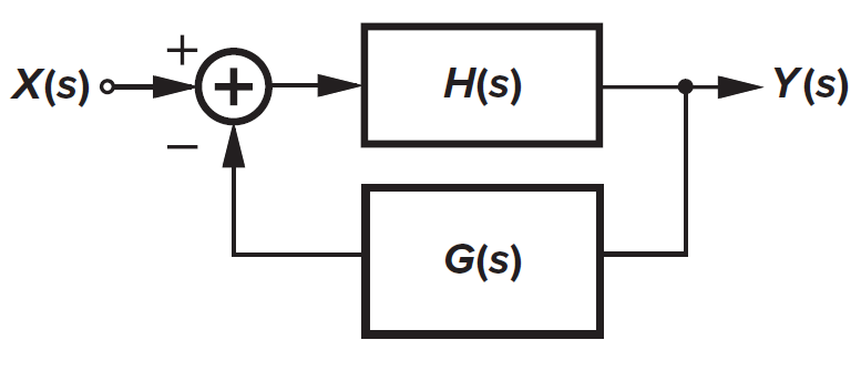
We call
This process indicates the equations below:
Both equations should hold at the same time to maintain the stability of the entire system. Combine the two equations and solve them
Generally,
This formula introduces some amazing properties:
Gain Desensitization:
Recall the CS stage we mentioned in the past. The AC gain is determined by
Then the total gain becomes (verify it with KCL and KVL)
Generally the intrinsic gain of a MOSFET
Now the gain is almost completely controlled by external components, more accurately because the variation of process and temperature do not change the cap.s.
In general, if the loop gain of the system
The loop gain
So how to find the loop gain? Obviously the loop gain operates on a specific signal in the circuit, so we should get rid of independent source to avoid their interference. Thus, the first step is setting the input as 0. The next step is to break the loop at some point and injext a test signal at the right direction. The follow the signal around the loop until it returns to the break point. We still take the CS stage with feedback as an example.
At node X, the signal is
Hence the loop gain is obtained by
Usually, we break the input terminal of the feedback network because it is usually the systematic output node.
Impedance Modification
Feedback also modifies impedance on the input and output terminals, and how the impedance is changed is related to the feedback topologies. On the output terminal, feedback network can sample voltage or current signal; On the input terminal, feedback network can also send back voltage or current as a feedback signal. The two selections on two terminals forms 4 topologies of feedback:
- Voltage - voltage: voltage sample, voltage back
- Voltage - current: voltage sample, current back
- Current - voltage: current sample, voltage back
- Current - current: current sample, current back
Voltage back is also called serial feedback and current back also called shunt feedback.
The conclusion is:
Voltage sampling reduces output impedance to
We prove voltage serial as an example. First setup an amplifier with gain
First comes the voltage serial feedback. To calculate the output impedance, eliminate the input (independent source) first.
The feedback network
indicating
As for the input impedance,
The relation is clear
giving
The amplifier input current is
obtaining
You can verify other topologies. But please remember that the gain and feedback coefficient may be dimensional when encountering voltage to current transformation. For example, if your topology is samping current and send back voltage, the dimension of your
But how to identify the feedback topologies? For voltage feedback signals you should connect them in series and for current ones you should do in parallel. This conclusion can be deduced easily through basic circuit laws.
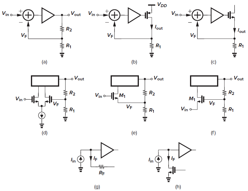
Here are some examples of the 4 feedback topologies.
Bandwidth Modification
Feedback pushes the pole to higher frequency regions and increase the total bandwidth of the system (usually at the cost of gain). Suppose the open-loop gain is frequency dependent and contains a 1-order pole
The closed-loop gain is also frequency dependent
Obviously, while the gain reduces to
Nonlinearity Reduction
Feedback also reduces linearity of the open-loop gain. Suppose the original open-loop gain is
Noise Performance: No improvements
Compared to the excellent properties above, the noise performance is not improved at all. Suppose in a typical voltage-voltage feedback loop the input-referred noise of the amplifier is
The total input-referred noise is still
Be aware that in most of the analysis above the output of interest is the same as teh quality sensed by the feedback network, but this is not always be the case. Take the example of the following circuit. In this circuit the sensed signal is at the source of M1 while the output is at the drain.
In such cases the input-referred noise of the closed-loop circuit may not be equal to that of the open-loop circuit even if the feedback network is noiseless. For simplicity, take only the noise of
The output
Then the input-referred noise caused by
In open-loop cases (gruond the negative input), the equations become
In this case noise performance worsens due to the feedback.
7.2 Problems of Primary Theory
In the last section we clarified the fundamental theory of feedback. However, we have neglected many factors, which may impact the result of our analysis. When it comes to cases that are not very ideal, for example the loop gain
The first problem stands for the leakage of the current to the feedback netowrk. In the primary theory, the feedback network is approximated with a infinite input impedance (voltage sampling for example) and absorbs no current from the output. However, in practice it must possess finite impedance. The extra absorption of output current must lead to a decrease of the open-loop gain. For example, the CS stage with a
In this circuit, the input of the MOSFET is no longer the direct input signal. Instead, the signal applied on the gate suffers from an attentuation due to the feedback network.
The second problem is that some circuit cannot be clearly decomposed into a forward path and a feedback network. In the following two stage amplifier, it’s ambiguous to distinguish whether
THe third problem is the noncanonical topology. The most used example is the source-degenerated CS stage. It has no loop at all.
The fourth problem is the bilateral paths in the loop. Some circuit may contain feedforward or backward flow paths. These mixed paths caused difficulty to the analysis.
The fifth problem is that some circuits contain s multiple feedback mechanisms, or we say multi-loops. For example, imagine a two-stage amplifier with a feedback, but the first stage is implemented by a source-degenerated CS stage. Then this circuit contains two mechanisms.
Due to these problems, we need some advanced theory for feedback: Two-port model and Bode’s method.
7.3 Two-Port Model Method
To solve the problems mentioned above, two-port models can be applied. Recall the two-port model in the fundamental circuit theory, there are 4 types of two-port models: Z, Y, G and H.
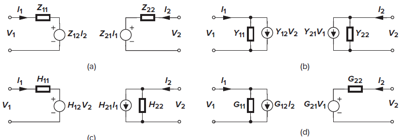
These four models are in fact combinations of Thevinen model and Norden model at the two ports. Each port includes a self-response compoennt and an interaction component. For example, Z model is composed with two Thevinen models. The left port satisfies
Here
All of the four can model all circuits modules. The key problem is: which one is the most suitable. In fundamental theory classes students always recite them. But in fact this is determined by the port property: We select proper model to avoid infinite impedance in serial connection and zero impedance in parallel connection.
Imagin a Thevinin source in you mind. If you want to express a low impedance port, you can just set the inner impedance to zero, and you obtained an ideal voltage source. But if you model the same port with a Norden model, you will have to short the current source and it becomes an independent system and fails to provide signals outwards. And the same for high impedance ports. A Thevinin model will bring an opened voltage source, which makes the model meaningless. Now we can raise the conclusion:
Thevinin model is suitable for low impedance ports, while Norden model suitable for high impedance ports.
Combined with out requirements: Voltage signals prefer high impedance input and low impedance output, current signals prefer low impedance input and high impeadnce output. You can determine which model you should apply according to the port property and the signal you desire to control.
Now we re-analyse the voltage-voltage feedback with two-ports model method.
Voltage in, voltage out, so we select G model. The complete model solves the bilateral problem. But the system will become too completed and in most cases these paths impacts nothing. So to simplify we ignore the bilateral terms
Then list the equations
Solve them
If we correspond the parameters with physical quantities in the primary theory, we get a mapping table:
The remaining terms,
If you rewrite the closed-loop gain, you will find the open-loop gain variation caused by feedback leakage
Clearly
By the way, since the G model gives
So to calculate the feedback network effect we can break the loop as follows:
This figure stands for the attenuation factor
Take the following example:
We can view it more clearly in two-ports figure.
Calculate the input and output impedance of the feedback network, then you will know how to break the loop. The final result is
For other topologies, the same analysis can be applied. We list the models and results in the following spaces in this section. But please note that the model selections are not unique. The voltage-voltage topology can also use an H model and a G model since the impedance are finite. There are no unique answer for selection, only the most suitable.
Current-Voltage Feedback
Note that in this topology the gain is dimensionalized as transconductance since it senses voltage and outputs current. So
Open loop
Voltage-Current Feedback
Also, the gain and feedback coefficient are also dimensional.
Open-loop
Current-Current Feedback
Open-loop
7.4 Bode’s Method and Blackman’s Impedance Theorem
Two port model method can still not deal with non-canonical types of feedback such as source-degenerated CS stage because it still decompose the feedback process into a forward amplifier and a feedback network. On the contrary, Bode’s method do not decompose feedback as a loop. Instead it views the entire circuit as a two-port circuit (the circuit do not need to include feedback), then choose a port inside the circuit:
Since the circuit is linear, all variables can be expressed with linear combinations of other variables. If the input is voltage signal (for example), the two equations must hold
To constraint a certain behavior, the circuit requires an external connection. In typical MOSFET circuit, the connection is usually
It seems meaningless to work on these undefined coefficient to calculate a solved problem. So what’s the advantage to come up with this “new” method? We should first think the physical meaning of the four coefficients.
The first coefficient,
In a traditional feedback loop, the feedback network absorbs no current so
Similarly,
They just shows the impact of one variable to another one. They cannot be decomposed as forward amplify, feedback or some other independent processes. In another word, the essense of Bode’s method is to “black-boxlize” the circuit and uses four coefficient to describe it.
Let’s view an example
Generally we take gate-source voltage as
Remember to disable the corresponding variable in calculation.
The most important application is to derive the Blackman’s impedance theorem. The circuit is still a black-box, but the output port is disabled. Instead the original input port serves as the “output port”.
We first introduce an index called return ratio. In the “black-boxlized” circuit, since there is no loop decomposed, the initial concept “loop gain” becomes meaningless. Instead, we use a similar concept called return ratio: Return ratio describes that when we inject a signal at one port with all independent sources disabled, how much the signal is amplified or attenuated (when frequency matters, there are also phase transition).
Now in the figure above, we select Bode’s equations as follows:
We can calculate the open-loop impedance when
This open-loop impedance is obtained without the feedback process. Then enable the feedback, calculate the total closed-loop impedance
Now leave the input port open, then
Then with external connection of
To simplify the expressions, we suppose the four coefficients are all positive and this circuit applies a negative feedback. Then the return ratio with the input port left open is
Second, we short the input port. Under this condition we have
and the shorted port return ratio is
Now compare and rewrite the closed-loop impedance expression
This equation is called Blackman impedance theorem.